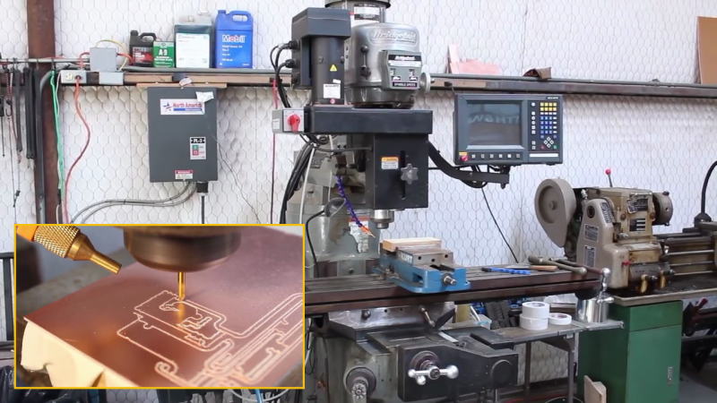
If you keep up with various retro vacuum tube projects, you probably have run across [UsagiElectric] aka [David]’s various PCBs that he makes on his own Bridgeport EZ-Track 3-axis milling machine — massively oversized for the job, as he puts it. In a recent video, [David] walks us through the steps of making a sample PCB, introducing the various tools and procedures of his workflow. He points out that these are the tools he uses, but the overall process should be similar no matter what tools you use.
- Logisim to validate logic designs
- TINA-TI, Texas Instrument’s version of the TINA SPICE simulator
- DesignSpark PCB for schematic entry and PCB layout
- FlatCAM, a computer-aided PCB manufacturing tool
For this video, [David] makes a half-adder circuit out of four vacuum tubes plus a seven-segment VFD tube to show the combined sum and carry outputs. Momentary switches are used to generate the two addends. Using this example, he proceeds to design, simulate, build and demonstrate a working circuit board. We like his use of the machined pin socket inserts for building a vacuum tube socket directly into the board.
Now this process isn’t for everyone. First of all, a Bridgeport mill is a pretty good sized, and heavy, tool. That said, these procedures should adapt well to other milling machines and engravers. We should point out that [David] is making boards mostly for vacuum tubes, where circuit trace width and spacing distances are generous. If you’re planning to make home PCBs for a 273-pin PGA chip, this isn’t the technique for you.
It seems that the bulk of [David]’s vacuum tube PCBs are single-sided, and reasonably so. They use wire links here and there to jump over traces. Adapting this process to double-sided PCBs is doable, but more complex. Are you milling double-sided boards in your lab? If so, let us know about it in the comments below.


“First of all, a Bridgeport mill is a pretty good sized, and heavy, tool. ”
I, would, say you, have a, problem with, punctuation.
Not if it’s being performed by William Shatner…
Not if you read “and heavy” as an interjection – A bridgeport is a pretty good sized and heavy tool. Then the commas make sense.
I thought 1 + 1 = 10
Nah! 1+1 = 11
:-)
Nah, 1 + 1 = Carry!
All I’m doing here is using some diode logic to illuminate certain segments on the VFD depending on whether Sum is high or Carry is high.
@Glaskows said: “I thought 1 + 1 = 10”
Depends on who’s running.
Flatcam is of great help and allow for double sided jobs thanks to addition of centering pins that allow for near-perfect match of two sides. I also found an utility that produces a probing G-code and automatic correction of PCB flatness default directly in your routing G-code, which is of great help too to keep consistent engraving depth (and thus width).
I experimented with FlatCAM in the beginning, but soon found the many, many clicks to do a board (that had to be repeated every time) a nightmare. PCB2Gcode has me drilling the centering pins by hand, but everything else is preconfigured and generating the gcode is just a drag’n drop away. The flatness on this mill is solved by a spring loaded z-axis and a glide shoe. It is always pressed onto the pcb and the mill depth is set by setting the glide shoe.
That’s good to know! I haven’t done any dual sided stuff because I tend to use the entire PCB surface area available as much as I can, which doesn’t leave any space available for some centering pins. But also, for the designs I do, the limiting factor is not usually trace density, but through hole component density. It turns out, resistors and capacitors take up quite a lot of space!
Our mill actually does have the ability to hook up a probe for leveling, but I’ve found the wood surface is surprisingly level after flattening it with the big bit. I’m sure if I were doing 0.6mm traces and SMD stuff, I’d run into issues with Z depth stuff, but at that point, the big old Bridgeport may not be precise enough anyways.
The way our setup at work is designed, you put a full 600x600mm sheet down on the two pins, and mill your much smaller board out, flip the large board on the pins, and mill the bottom side, then cut it out with a router. That handles alignment and gives excellent pcb usage if you’re willing to spend the time aligning multiple jobs.
That’s not an EZ-Trak btw… it’s a Bridgeport with an Acu-Rite MillPWR controller.
You’re right that it’s an Acu-Rite MillPWR controller, but the mill itself is definitely an EZ-Trak. It literally says it right on the side. If you look at 16:07 in the video, I show a close up of the EZ-Trak plaque.
The workflow I have figured out for me is Kicad for the PCB, export to gerber. Then use PCB2gcode to create movement files for the mill from said gerbers. It supports double sided along a mirror axis – which means manually controll the machine to drill through the pcb into the support material (HDF) in at least 3 places symmetrically to the mirror axis and insert location pins in these places, so the pcb can be flipped in place after milling one side. Yes these holes need to be drilled a new every time.
To mill multiple projects at once the GerberPanelizer from ThisIsNotRocketScience is very usefull. Sadly it is the only part not buildable in Linux. The finesse in using PCB2gcode comes not from the (very) outdated GUI, but from a premade config file and a windows batch file. You put the batch and config file into the kicad project folder and drag’n drop the kicad project file onto the batch file and it automagically supplies all the file names, paths, etc. to PCB2gcode. The cherry on top is the mill runs LinuxCNC, so OSS all the way through.
All looks quite good.
I noticed that the milling machine has a port to blow the (silica) dust away.
It really needs a vacuum or wet cutting. Silicosis (or even lung cancer) is probably worse than exposure to asbestos.
I just coat the PCB in a not too-heavy oil before engraving. Enough to coat the surface but not enough for it to flow away. It causes the dust to stick and increases the life of the engraving bit. No other modification necessary. For drilling a vacuum is better suited.
Nice! I’m going to remember that when I finally get started.
You can also use FR-1 blanks, which don’t use fiberglass. FR-1 is a bonded-paper board, and it’s much safer to mill than FR-4.
That’s a good idea!
Since the mill is out in the very well ventilated garage, I usually just leave as soon as the cut starts and just chill in side until a few minutes after the cut has finished. Then I go around with the vacuum and suck up all the dust that has settled on and around the machine.
But, the thin layer of light oil on the surface makes a lot more sense, and I like the idea of better longevity for the engraving bit. I’ll have to try that in the future, particularly for some of the massive PCBs I’m going to be cutting (500mm x 100mm).
On both my work and home systems, the spindle head is sprung so it glides on the surface of the material, and the area around the bit is enclosed so when it’s down and drilling/milling, a vacuum system pulls the head down onto the material and evacuates all the drilling dust. Note this can be a pita as the vacuum hose gets pulled around a lot, and sometimes fails or pulls off the head.
Precisebits sells a fluid (not to mention every other cutter/tool) for doing PCBs for exactly this reason.
https://www.precisebits.com/products/chemicals/MELube.asp
There is a video showing how it works.
Fiberglass is amorphous; silicosis is not a concern
Those engraving and drilling bits prefer 10,000+ RPM … not <3000 RPM. Probing the surface of the board is critical to getting a reproducible workflow. That said, this board turned out pretty good.
Absolutely right here!
But, you work with what you got, right? I happened to have a Bridgeport CNC in the garage, so I figured why not give it a go. I seem to have found a pretty good balance of spindle speed and feed speed, and the results are surprisingly reproducible. I’ve cut hundreds of boards so far for various projects and they all turn out pretty good. My entire vacuum tube computer was built using this exact same construction technique!
I built an offset adapter to be able to run a compact router that turns up to 23k rpm, just to be able to run the tiny bits at decent feed rates. I have a Supermax with LinuxCNC and oddly enough every time I have used it its only to build another tool to use on the mill.
There’s an _old_ linux utility called gEDA, that is an integrated schematic editor/pcb layout software, with roots back in some Atari pcb software, that’ll directly produce gcode. I’ve used it successfully, although I can’t really recommend the schematic/pcb layout software as being great. (It’s not terrible, but making footprints is a chore.)
I routinely use gEDA (gschem, pcb) and its “Export… gcode” feature, which I prefer over pcb2gcode. Its “Export, gerber” output goes straight to the fab for prettier boards, so I’ve no need to learn newer tools. Though I agree that footprints take work. To ease the pain, I use Ruby to generate mine procedurally.
pcb is not really mantained anymore and will be harder to install as it bitrots. Have you ever tried pcb-rnd? It also has improved g-code export.
I’m currently working on my workflow for milling PCBs at home and I can recommend or give tips for my approach only using KiCAD and FreeCAD to generate DXF or GCODE.
I used to create some pcbs using a cheap chinese laser engraver and photo sensitive pcb material. The laser beam is very fine and developping the uv sensitive material works very well. Next I used a semi prfessional spray etching machine that heated the ferro chloride to 40 degrees celcius. It only took 2 minutes to etch away the isolation traces that had been lasered. Due to the fact only minimal photosensitive material and cupper needed to be removed, the development and etching baths could be used a very long time.
Does anyone have the latest install of Flatcam? (FlatCAM_beta_8.994_x64_installer.exe), the link from bitbucket seems to be down (points to an s3.amazonaws.com url, that times out.)