We all know the havoc that water in the wrong place can do to a piece of electronics, and thus we’ve probably all had devices damaged beyond repair. Should [Solderking] have thrown away the water-damaged PCB from a Nintendo Pokemon Ruby cartridge? Of course he should, but when faced with a board on which all vias had succumbed to corrosion he took the less obvious path and repaired them.
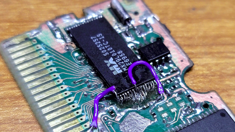
Aside from some very fine soldering in the video below the break there’s little unexpected. He removes the parts and tries a spot of reworking, but the reassembled board doesn’t boot. So he removes them again and this time sands it back to copper. There follows a repair of every single vial on the board, sticking fine wires through the holes into a sponge and soldering the top, before turning it over and fixing the forest of wires on the other side. Fixing the ROM results in a rather challenging fitment involving the chip being mounted at an angle and extra wires going to its pads, which demonstrates the value in this story. It’s not one of monetary value but of persevering with some epic rework to achieve a PCB which eventually boots. Of course a replacement board would make more sense. But that’s not the point, is it?


I wonder if it was just a few vias that needed replacing. Though this works if you gotta catch them all.
Planned obsolescence? Past HaD articles showed many issues with battery powered cartridges mitigated with FRAM.
https://hackaday.com/2021/11/08/pokemon-time-capsule/
Today FRAM is cheap enough, if happy customers are your intention.
I’ve had the opposite experience, in needing to replace a failed FRAM chip on a Sonic 3 cartridge. (Plenty of these cartridges now have failed FRAM chips and won’t save progress.)
Was the soldering temperature okay? It shouldn’t really happen. Even if you use a few powers of ten in lifetime. Even EEPROM should be fine if there is no constant writing and a save every hour or so. Just say, 1 million saves should be enough. I cannot even imagine 10^12 saves or 10^14 saves which the Japenese (Toshiba?) and the Americans (Cypress) advertise for their space magic storage.
I typically repair damaged vias by flood filling with solder. Just remove the solder mask around the connecting traces and place some flux down and let the solder wick. Usually pretty easy.
I was hoping for a more methodical approach in the video. E.g. find bug > fix bug > repeat until device works. For this repair, you’ll never know if it was a single broken via or a dozen, same for the second iteration. While debugging takes time, the process is more efficient than just repairing everything.
Another one many people miss, is they turn on the device to see if it works and then start repairing. In this process you are quite likely to break more parts than when you would inspect and clean before powering the device.
OK, this shows something that I’ve noticed on GBA/GBC and the Googles don’t seem to know the answer;
On the Cartridge PCBs, there are often a number of through board holes, many of them Intersecting tracks.
These can be clearly seen on the Photos in this set. One near the top of the IC under the backup battery, another just above the cart interface pins, another up near the RTC/SRAM IC.
I’ve seen this on lots of Cart PCBs. The only explanations I can think of are board fixes/modifications to correct manufacturing errors (but surely they would have re-spun the biggest selling GB games?) or to disable test functionality after manufacture/programming (very risky surely to be drilling a PCB after manufacture?).
Anyone chime in with any better explanations for me? Been driving me mad for years!
Those lines are connected together so they can electrically gold plate the PCB. Then they drill them so they are no longer shorted.
“There follows a repair of every single vial on the board” – Vial?
Just a typoe.
interesting technique, and the cart is reasonably common enough that if the PCB is destroyed during the repair, it can be replaced. (I think?)
>Of course a replacement board would make more sense. But that’s not the point, is it?
I don’t think it’s up to hackaday to pass judgement here, and stop-and-go work does take a lot of the flow out of a weekend project, turning it into a two-consecutive-weekends task with extra expenses for a replacement PCB after doing the menial task of re-creating the board, or at least processing some files (though that workflow may be interesting to watch).
If there’s one sin in this project, it’s to skip creating high-resolution PCB images for someone else to pick it up, and maybe finish the PCB resurrection. Luckily there is a front-side picture, but the frame at 2:49 is unusable. So that’s an entire branch of possibilities cut off, which I find annoying.