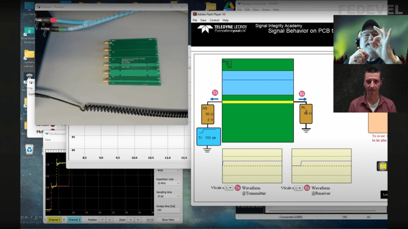
PCB design starts off being a relatively easy affair — you create a rectangular outline, assign some component footprints, run some traces, and dump out some Gerber files to send to the fab. Then as you get more experienced and begin trying harder circuits, dipping into switching power supplies, high speed digital and low noise analog, things get progressively more difficult; and we haven’t even talked about RF or microwave design yet, where things can get just plain weird from the uninitiated viewpoint. [Robert Feranec] is no stranger to such matters, and he’s teamed up with one of leading experts (and one of this scribe’s personal electronics heroes) in signal integrity matters, [Prof. Eric Bogatin] for a deep dive into the how and why of controlled impedance design.
One interesting part of the discussion is why is 50 Ω so prevalent? The answer is firstly historical. Back in the 1930s, coaxial cables needed for radio applications, were designed to minimize transmission loss, using reasonable dimensions and polyethylene insulation, the impedance came out at 50 Ω. Secondarily, when designing PCB traces for a reasonable cost fab, there is a trade-off between power consumption and noise immunity.
As a rule of thumb, lowering the impedance increases noise immunity at the cost of more power consumption, and higher impedance goes the other way. You need to balance this with the resulting trace widths, separation and overall routing density you can tolerate.
Another fun story was when Intel were designing a high speed bus for graphical interfaces, and created a simulation of a typical bus structure and parameterized the physical constants, such as the trace line widths, dielectric thickness, via sizes and so on, that were viable with low-cost PCB fab houses. Then, using a Monte Carlo simulation to run 400,000 simulations, they located the sweet spot. Since the via design compatible with the cheap fab design rules resulted often in a via characteristic impedance that came out quite low, it was recommended to reduce the trace impedance from 100 Ω to 85 Ω differential, rather than try tweak the via geometry to bring it up to match the trace. Fun stuff!
We admit, the video is from the start of the year and very long, but for such important basic concepts in high speed digital design, we think it’s well worth your time. We certainly picked up a couple of useful titbits!
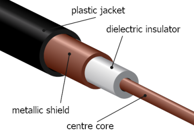
Now we’ve got the PCB construction nailed, why circle back and go check those cables?


tell me why path si small, not fat if it is possible?
many times i see small path when is possible change it to bigest , bigest path less impedance
Lazy (or ignorant) designers is what I attribute it to.
Looks like most of the discussion is about RF, where PCB traces are essentially waveguides. So now the fatness is determined by the signals wavelength and the required impedance rather than current. The fatness will give a lower resistive impedance but could alter capacitance and inductance which is now more important at RF as this can change the frequency content of the signal. There is also more to think about with coupling, skin effect with RF magic. If routing a DC power trace then most likely you’d want a nice fat one.
Impedance is not resistance.
Wide traces have lower resistance to DC currents than thin ones. Their impedance to AC signals is a whole other thing.
It becomes relevant once your traces are long enough to be considered transmission lines.
For most small PCBs most signals are short enough that actually the impedance won’t matter most of the time.
For bigger PCBs and anything with usb2 or higher (pcie, mipi, etc) if you don’t worry about impedance you could have problems.
Most of the problems are EMC related though if you have analog stuff (audio or ADC) you can get into a real mess.
It’s common misconception that it’s only relevant to RF. It’s a real problem even on Arduino level designs.
I used to think that 50 Ω microstrip traces on circuit boards are just the result of following the standard of the RF industry, and there’s no reason why a 30 Ω or 75 Ω microstrip trace can’t be used. But later, I’ve heard some good justifications for 50 Ω and why this ancient industry standard (originated from air coax cables of the 1930s) can actually still make sense today, by a happy coincidence.
> The question is often asked, why do we use 50 ohms for the impedance of PCBs? Why not use 60 or 75 ohms? The answer lies in the limitations of materials and processes and the layer requirements for PCBs. Figure 24.4 shows the impedance achieved with a 5-mil wide trace in the three types of transmission lines – surface microstrip, buried microstrip and stripline. The 5-mil trace width has been chosen as the narrowest trace width that is practical in volume manufacturing. The height above the nearest plane has been increased from 5 mils to 20 mils to see how high the impedance could be on each of these three layer types.
> Even with the narrowest production trace width, stripline layers cannot achieve high impedances. In all cases, high impedances require very thick dielectrics, making PCBs excessively thick, as well, and subject to severe crosstalk.
> If the only signal layers in a PCB are surface microstrip, it is possible to have impedances ranging from 65 ohms to 113 ohms. 50 ohms would be possible only if the height above the plane were reduced to less than 5 mils, possible, but on the low end of practical material thickness. As soon as more than two signal layers are needed, the additional layers will have to be buried microstrip or stripline. If buried microstrip is chosen, the possible impedances range from 58 to 101 ohms, so the highest impedance that could be achieved is still quite high. However, adding the buried microstrip layer would force the surface microstrip layer farther away from the plane and it would be dif- fi cult, if not impossible, to make the impedance of these two layer types the same.
> If four or more routing layers of the same impedance are needed, all but two of them will have to be stripline layers. In this case, the possible impedances range from 42 ohms to about 80 ohms. So, it would be possible to create a PCB with signal layer impedances up to 80 ohms. However, to do this the dielectric thicknesses would have to be very large. This would result in a very thick PCB. As will be seen in a later chapter, the crosstalk would also be excessively high.
> Bearing in mind the constraints of crosstalk and reasonable PCB thickness, dielectrics should be kept under 6 mils. With this constraint, it is not possible to achieve impedances higher than about 55 ohms on stripline layers. This will force the im- pedance on the buried microstrip layers to be the same. As experience is gained in creating PCB stack ups that balance the needs of manufacturability, crosstalk and impedance against each other, it will become clear that 50 ohms is the best compromise. Other impedances, higher and lower than this, will be difficult to achieve. If a 38-ohm impedance, such as that required by Rambus™, is used, manufacturability will be compromised and if the 65+ ohms required by some protocols is used, crosstalk will be excessive.
– Right the First Time—A Practical Handbook on High-speed PCB and System Design, Chapter 24: Methods for Calculating and Measuring Impedance, by Lee W. Ritchey,
Robert Feranecs channel is always worth visiting. There’s an awesome video/interview on high-power trace design and lots of other good stuff, too. Highly recommended! (Title: Do you need thick copper layers in PCB for high currents? Are you sure? | Steve Sandler)
Robert Feranec seems like such a knowledgeable guy and he does some great explanations/visualisations but I struggle to watch a very slow talking 50+ minute video on some wrinkle of PCB design each time.
If he did more <5 minute ones that just give you the basics/overview without the rambling / deep-dive I think he'd get a lot more views.