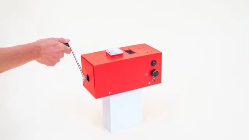
A common complaint about the rise of commercial AI services is that they are power-hungry and thus damage the environment. If this concerns you then [Squeezlabs] has the solution, in the form of an AI powered by a handcrank.
The guts of the system is a Raspberry Pi 5 running llama.cpp and appropriate speech conversions, but it and the Large Language Model (LLM) side are not the most interesting part of this system. The power comes from a hand crank charger of the type you’ll see for sale on the likes of AliExpress, designed for USB charging. That in itself is not enough to power the Pi though, as upticks in the processing can cause brownouts that crash the machine. Thus there’s a custom-made capacitor board to take up the strain, and even with that the handle resistance varies significantly depending on the computing load.
We can see that this is not the ideal way to experience an LLM, but maybe that’s not the point. It does however point towards a future in which the power demands of processing decrease and less effort is required. Meanwhile, this is by no means the first hand cranked project we’ve seen.


Neat project/installation :)
I guess it’s not also trained using the crank as as energy input?
Of course! Otherwise the adjective “truly” wouldn’t be warranted!
Obviously not… The training was powered by hamsters running in wheels.
I wouldn’t make bets on computing better becoming maybe more than another 10x or so better. The latest headline figures from TSMC are 1.6x improvement per generation, not 2x, and that number is trending down. And you get 1.6 perf at the same wattage, or 1.6 wattage reduction at the same perf, not both as in the heady days of pre-2005 dennard scaling. A future is visible where doubling happens every 20 years instead of every 2.
We’ve run out of road. We shrank transistors until we couldn’t shrink them anymore. Then we started optimizing their geometry, moving from planar transistors at 28nm to finfets, to forksheets, to stacked single-atom-thick gate-all-around nanosheets in the next generation or two. Then as that ran out we tackled more obscure inefficiencies, implementing tricks like silicon interposer advanced packaging, more radical litho pattern geometry optimizations, backside power delivery, and soon CFETs where we get more areal density by stacking the complementary N-channel and P-channel transistors on top of each other. That last one is the current end of the roadmap, and you’ll notice it gets you more density but doesn’t do as much for power dissipation. The ultimate step is projected to be manufacturing the N and P transistors on different wafers and bonding them together, just to exploit slightly different crystal alignment for each type.
Huawei has been a surprise entrant with layered logic layout and chip stacking, but while this reduces buffers, cuts some power dissipation, and raises clocks, this is another side trick. It wont be long before it’s replicated by other fabs (limiting factor: large-scale software rewrites and precision die placement+bonding), and it isn’t a viable roadmap after we master it in the first couple of generations.
computing becoming*
Oh, and worth mentioning are the litho machines. We’ve taken on EUV litho, then high-numerical-aperture EUV, and ultra-high NA EUV is in the works. But ASML themselves have admitted that pretty soon it’s not going to make sense to keep chasing this further, simply on an economics basis. you’ll never turn a profit with how much the machines will cost and how many wafers you’ll be able to process per minute.
time to switch to different materials like GaAs or InP. way more expensive but ALOT faster transistors.
Nah, there’s lots of potential in graphene/silicene, optical computing, optronics.
Not really. Graphene is what those single-atom-thick nanosheets are made of. Optical computing isn’t significantly faster because the speed of light in glass is about the same as the speed of EM field propagation through existing wiring. It’s also handicapped by the lack of viable alternatives to the transistor. Decades of searching, and the best candidates are worse than the first BJT.
but…… QUANTUM COMPUTING!!
Fraud. https://eprint.iacr.org/2025/1237
Particularly for AI, computing energy requirements will decrease when more specialized chips start to be made. It’s also massively parallel, so there is no real limitation on computing capacity other than the energy and chip costs.
Regarding Moore’s law, 3D chips are the next direction. Power dissipation will need to be limited, but on the other hand interconnect distances are shorter. It might even be possible to have tiny cooling channels going right through the chip, with MEMS pumps and all.
It depends on what you mean by AI. Language models are essentially emulating parts of the “slow brain” abstract mode of thinking that draws on large datasets and information compression, which hits limits in data transfer rather than how fast you can compute it. Memory, bandwidth, and access time has always been more limiting and costly in terms of parallelization, especially when it comes to random access rather than processing streams of data.
This is just simply wrong.
Not only are LLMs nothing like how the brain works and contain no structures in common with real neural circuits (you will find no transformers in the brain) but our entire paradigm of neural network machine learning is based on a process (backpropigation) which is known to be physically impossible in biological brains. The current best theory for how biological brains operate is called Predictive Coding, which is a complex dynamics system that isn’t well suited to simulation on a computer. (yay, N-body physics!)
The datasets used to train LLM also simply do not exist in LLMs. The finished product is a probability mapping between the last N tokens and the next token, nothing more. There is no abstract thinking and no database lookup, just extracted probabilities being sampled to give the next few letters of text. There have been crude attempts to emulate abstract thought on top, by asking models to generate a textual justification (reasoning models) but see above for how this “tokenmaxing” approach has ballooned compute costs far faster than hardware has been able to keep up.
Have you looked at any of the real world trends? Computing energy requirements are going UP not DOWN. The perf-per-watt may be improving slightly (see the above 1.6x figure) but AI compute CONSUMPTION has been increasing rapidly, especially in watts-per-query due to “tokenmaxing.” (the approach of throwing more tokens at the wall to try and get higher quality output, eg. mixture-of-experts, AI “councils” etc)
3D chips compound the problem even more, because if you can’t reduce the per-transistor power draw then stacking the chips just means making more heat in a smaller package (making cooling overall harder) while also making heat transfer through the ship less efficient.
As for cooling channels in the chip, there simply isn’t any room. Any cooling channel large enough to actually carry fluids is far wider than entire sections of circuitry. Remember, fluid dynamics doesn’t scale down like you’d expect, and we’re decades deep into nanotechnology here.
“It does however point towards a future in which the power demands of processing decrease…”
I don’t think they were referring to magic future silicon in this context. The efficiency of AI is the limiting factor here. You can run Turing-complete Minecraft on 2 GB of DDR3 in Java, or you can run wobbly nightmare Minecraft at 20fps-360p on an H100 with 80 GB of HBM using a transformer-based world model.
What you’re describing would be an entirely new paradigm of machine learning. Throw out transformer-based large language models and pick something else, in other words.
That’s not my point. There are still more or less efficient examples of transformer-based language models.
I’m saying the software is the thing varying by orders of magnitude, and that nobody reasonable is expecting hardware to become dramatically more powerful.
Comparing between only transformer-based language models, you can still vary between hundreds of GB of VRAM or single digits.
Waiting for AI to suggest to put an engine on that crank…
Waiting for OpenClaw to order its own engine from Amazon…
The energy to operate this ultimately comes from the food you eat. Best case, that’s a few dollars per kilowatt hour.
So: How many tokens per pizza does it get?
Well, two points first:
1. You don’t eat you cease to be, without you no question would be asked. You eat no matter what. So, how much additional eat is needed to power that crank, should be the question. (This should be written Douglas Adam’s style)
2. Energy for the food mostly comes from the sun.
Ok:
“The human body operates at roughly 20% to 25% mechanical efficiency. This means only one-quarter of your food calories translate into movement, while the rest dissipate as body heat.”
“Fuel-burning to electricity efficiency generally ranges from 33% to 60%. It varies depending on the fuel type and the technology used. Most traditional power plants lose about half to two-thirds of their original fuel energy as waste heat.”
So, the power plant, technically, wins. But “Idling Human consumes 100 watts anyways”
A human turning a crank consumes more than 100 Watts.
Food production is also an energy sink:
https://pmc.ncbi.nlm.nih.gov/articles/PMC11650529/
So, the EROEI corrected efficiency of a human turning a crank is roughly 18-23%
Some estimates that also account for food waste and distribution etc. in the US can put the EROEI figure all the way down to 0.1 which means 1-2% efficiency in using human power to turn a crank.
Of course it depends largely on what you eat. If you eat only oatmeal porridge that you grow out of your own back yard, you can still be a net energy producer by a good margin.
if you eat factory-farmed beef/pork/chicken and that is the source of your hand-cranked power, i don’t think it’s very environmentally-friendly AI
How long until the AI convinces the human to keep cranking the handle and when does this become a symbiotic relationship?
“this is not the ideal way to experience an LLM”
I beg to differ.
“I told them it means peace amongst worlds….How hilarious is that?”
when i was 17 in the late 20th century, i had a small fleet of obsolete computers that had been gifted to me. So I used a 16MHz 386 with 2MB RAM for two stupid ‘because i can’ hacks. I made a shim between the svgalib API and libaa (ASCII art), and i set it up as a dumb terminal and played quake on the 386 over a serial link to a bigger computer. Then i set up netboot and swapping over SLIP, and built a kernel (version 1.2.13) on it (it took days).
The former hack became ttyquake and perhaps an early example of the ‘can it run doom’ meme. The latter example happened in obscurity. But i never used that 386 again…i never played quake on it or used it as a build host.
I’m not sure what makes a hack notable and i guess this just shows my age / cynicism, but “i can run doom / linux / llama on it” just kind of makes me sad these days. When the wind blew from “i can’t get a computer for anything” to “i can have an old computer for free”, that was a miracle to me but computers are everywhere now. “my pi can run software” doesn’t energize my soul. i wish it did.
Not stupid, IMHO. It made sense. By early 90s, software such as Windows or GeoWorks Ensemble easily wanted 2, 4 or more RAM – no matter the CPU.
And that’s not considering the commercial applications and the user data, even.
2 MB weren’t much anymore by ca. 1992-1994 or so, I think.
1 MB 30 pin 8-Bit SIMMs were common at the time, also, I think.
So on a 386 you need a pair of 4 SIMMs because of 32-Bit data bus of the 386 (equals 4MB).
On a 286 or 386SX, you just needed a pair of 2 SIMMs because of 16 Bit data bus (equals 2 MB).
Throwing 256 KB SIMMs into the mix was possible, as well, but they were kind of obsolete by that time. And slow, often. >80ns.
Motherboards back then had 4 to 8 SIMM slots, I think.
Speaking of motherboards, many 286 motherboards supported up to 4 MB, also.
So 4 MB of SIMM based RAM was the “full” memory expansion here.
To get more, up to 16MB of Extended Memory, memory boards for ISA bus could be used.
They existed since the days of the IBM PC/AT model 5170.
@GregA my bad, I didn’t correctly read your comment. Nice hacks, also!
With the computing power available at the time, the trick was to make it do anything interesting at all. What is impressive today is that a hand-cranked computer can produce natural speech and actually answer to spoken language in a sensible manner, in real time, with commercially available language models that are not exactly optimized for the purpose. That’s something that would have been total science fiction back in the day of a 386.
A story comes to mind. In the early 20th century, when explorers went around East Asia and found indigenous people living in the islands, the captain of an expedition tried to impress a local chieftain by showing off their airplanes. The chieftain was not phased, saying, “You can make fire out of your fingertips, of course you can also fly”, referring to the fact that they had matchsticks.
When the technology is that much beyond our conceptions, we fail to appreciate its gravity. Magic is just magic.
Or, another case: some member of the Royal Academy whose name I forget, commented on an early demonstration of radio transmission: “That’s just induction. Nothing new.”
Easier would be to train a parrot.
If this used a stationary bike for power and required an entire workout before output it would at least be useful…
Right now it is just the wort of computing while also being a waste of hardware and calories, all to get an undeserved pat on the back.
Hamster generator can help