As electronics have advanced, they’ve not only gotten more powerful but smaller as well. This size is great for portability and speed but can make things like repair more inaccessible to those of us with only a simple soldering iron. Even simply figuring out what modern PCBs do is beyond most of our abilities due to the shrinking sizes. Thankfully, however, [μSoldering] has spent their career around state-of-the-art soldering equipment working on intricate PCBs with tiny surface-mount components and was just the person to document a complete netlist of the Nintendo Switch through meticulous testing, a special camera, and the use of a lot of very small wires.
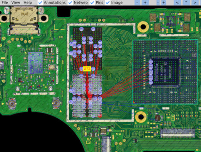
 The first part of reverse-engineering the Switch is to generate images of the PCBs. These images are taken at an astonishing 6,000 PPI and as a result are incredibly large files. But with that level of detail the process starts to come together. A special piece of software is used from there that allows point-and-click on the images to start to piece the puzzle together, and with an idea of where everything goes the build moves into the physical world.
[μSoldering] removes all of the parts on the PCBs with hot air and then meticulously wires them back up using a custom PCB that allows each connection to be wired up and checked one-by-one. With everything working the way it is meant to, a completed netlist documenting every single connection on the Switch hardware can finally be assembled.
The final documentation includes over two thousand photos and almost as many individual wires with over 30,000 solder joints. It’s an impressive body of work that [μSoldering] hopes will help others working with this hardware while at the same time keeping their specialized skills up-to-date. We also have fairly extensive documentation about some of the Switch’s on-board chips as well, further expanding our body of knowledge on how these gaming consoles work and how they’re put together.


I know this isn’t directly related to computer security, but the lesson is clear: never underestimate the resourcefulness of someone with lots of free time and dedication to a task.
Ambitious a.f., i love it.
What is this mysterious software used ?
The world needs a good reverse-engineering tool that can map a pcb from photos all the way to a schematic. That´s one task AI could be good at.
+1 would love to know as well
In the blog it is referred to as openboardview
There might be a possibility of automatizing this, with some computer vision to detect the pads and some kind of dual actuator to position the probes. Though it gets harder if there are components on both sides of the board.
I believe the professionals just X-ray the PCB
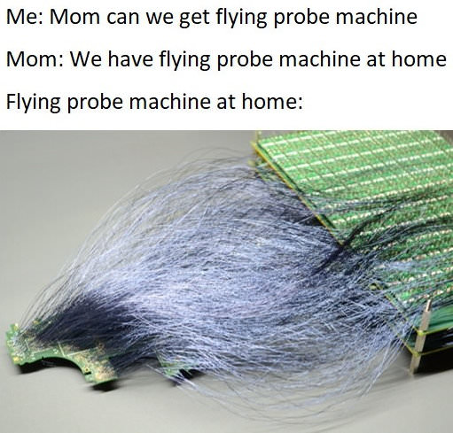
Yes, this is known as a “flying probe machine” as referenced in the image.
I thought about using computer vision and slowly grinding away PCB material.
That way you could see traces, buried vias etc and where each component is connected.
Sadly, my skills lack in this field :)
Similar to a CT scan, or the reverse of a 3D printer slicer…
Yes, I was thinking about such a machine – it would basically wet grind the PCB under an angle – so that the scanned view is basically a narrow band. You do not want to do it at 0 deg or 90 deg cut – as the features you are interested in are in that orientation – so my idea was to grind it in a 30 (or 60) deg angle, or even less – to clearly identify the vias that may pass just to some layers.
There is actually a similar thing to image organic things like tissues – the machine basically cuts off thin layers and the whole process result is a volumetric capture.
eek all those black magic wiggly traces in the middle. How did they ever get it to work!?
That’s… a lot of work…
Why not just scan the assembled board on both sides, remove components and scan each layer, lapping the PCB to access the inner layers.
Then import the images into a PCB app and trace it all out to a schematic?
That’s only good up to two layers.
If you google ‘PCB reverse engineering services’ (Sierra, RAYPCB, etc.), you’ll see several companies that offer engineering services for this exact thing. They document everything on the outer layers, shave the board down until the inner planes are exposed, and use images from the process to determine the overall netlist. Not sure if there’s a limit on how many layers you can have but each of the sites I mentioned have explanations for how they process 4 layer boards.
Damn impressive work, and probably well timed as I doubt the switch has much life left in it for its intended use, but the hardware is actually still pretty decent. I wonder how many revisions of the PCB and BOM there have been, presumably they would have strong familial resemblance but could be more than different enough to be difficult to use this info to do what you want.
Probably at least 4. Early, late, Lite and OLED. Although the hardware is basically a Nvidia Shield/Jetson devboard, so I’m sure some of the work would translate.
You can apparently get 3GB and 4GB memory chips to go up to 6GB/8GB system memory, not too expensive either.
I haven’t quite done BGA level reversing, but to some degree yes. Since I work at a PCB fab and have access to few flying probe testers, I can reverse the traces and pads from scanned images and then make a test file that will test shorts between all test points on the board. Then I can use this error report to augment the initial netlist to reflect the real world netlist. Its a long test, but still, its automatic.
Kind of speechless at the level of work done to get this out to the world, especially as it’s not using the tools of the professional trade.
The sheer number of hair-fine, physical connections is terrifying to see at first, but this work is beautiful.
And it’s all useless because Nvidia refuses to release a graphica driver for Linux that doesn’t have a bug where the render driver goes through a glitchy pipeline resulting in poor to unusable fram pacing when you are using a rotated screen (I guess a hardware fix might be finding a native landscape screen, but I’m sure Nintendo would have done that if it was possible).
But still hoping. Cool setup
I think this guy may have ‘hacked’ himself a business. Good job!