As electronics have advanced, they’ve not only gotten more powerful but smaller as well. This size is great for portability and speed but can make things like repair more inaccessible to those of us with only a simple soldering iron. Even simply figuring out what modern PCBs do is beyond most of our abilities due to the shrinking sizes. Thankfully, however, [μSoldering] has spent their career around state-of-the-art soldering equipment working on intricate PCBs with tiny surface-mount components and was just the person to document a complete netlist of the Nintendo Switch through meticulous testing, a special camera, and the use of a lot of very small wires.
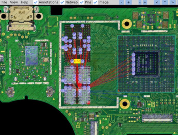
 The first part of reverse-engineering the Switch is to generate images of the PCBs. These images are taken at an astonishing 6,000 PPI and as a result are incredibly large files. But with that level of detail the process starts to come together. A special piece of software is used from there that allows point-and-click on the images to start to piece the puzzle together, and with an idea of where everything goes the build moves into the physical world.
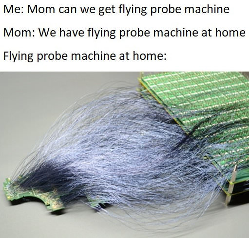
[μSoldering] removes all of the parts on the PCBs with hot air and then meticulously wires them back up using a custom PCB that allows each connection to be wired up and checked one-by-one. With everything working the way it is meant to, a completed netlist documenting every single connection on the Switch hardware can finally be assembled.
The final documentation includes over two thousand photos and almost as many individual wires with over 30,000 solder joints. It’s an impressive body of work that [μSoldering] hopes will help others working with this hardware while at the same time keeping their specialized skills up-to-date. We also have fairly extensive documentation about some of the Switch’s on-board chips as well, further expanding our body of knowledge on how these gaming consoles work and how they’re put together.


