
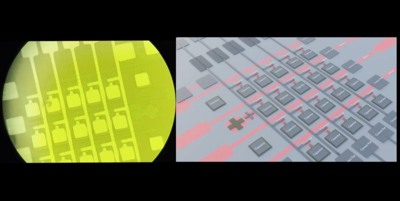
There’s little point in setting up your own shed-based clean room for semiconductor purposes if you don’t try to do something practical with it. Something like responding to the RAMpocalypse by trying to make your own RAM, for example.
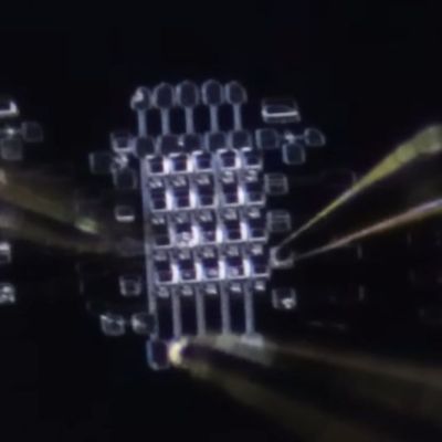
After all, what could be so hard about etching the same repeating structures over and over? In a recent video, [Dr. Semiconductor]’s experience doing exactly this are detailed, with actual DRAM resulting at the end.
We covered the construction of the clean room shed previously, which should provide at least the basic conditions to produce semiconductors without worrying about contaminating dies. From here the process is reminiscent of etching PCBs, with a prepared surface coated with photoresist. Using UV exposure through a mask, the pattern is etched into the photoresist and from there the pattern is subsequently etched into the wafer’s surface.
With the patterns formed, the next step is doping of the silicon in order to create the active structures, i.e. the transistors and capacitors. Doping can be done in a variety of ways, with ion implantation being the industry standard method, but a bit too expensive and bulky for a shed fab. Instead a spin-on-glass method was used. After this the remaining functional structures can be built up.
If anyone was expecting to see a DDR5 DRAM die pop out at the end, they’re bound to be disappointed. The target here was to create a 5×4 array of DRAM cells, for a dizzying 20 bits. Still, the fact that it’s possible to DIY DRAM like this at home is already pretty awesome, with clearly plenty of room to push it towards and past fabrication nodes of the 1990s and beyond.
Although the produced DRAM cells have fairly leaky capacitors, they’re good enough for their purpose, and the plan is to scale up to a large DRAM array from here. Whether the DRAM control logic will also be implemented in hardware like this remains to be seen, but the video’s ending makes it clear that the goal is to attach it to a PC somehow.









Just a step above rope memory.
I tried to make one out of chicklets once…and this goth girl ate it….but she can do calculus once I give a piercing of hers a good twist.
All HAMs need a Goth inni button for cables…nipple rings for controls.
2X-2L…come in please…all the ships at sea…
I wish I was illiterate
: | this is correct
Oi, USA flew to the moon on rope memory.
This inspired me to sketch up a DRAM module in discretes. It comes out to about 64 bytes per 10 cm square board, for about a penny per bit. 1 kB per liter for about $100.
Cool, please tell us more about this project/concept. It may not be much performance wise but it certainly is inspiring and lot’s of fun to learn about DRAM technology from the ground up.
Not much to it. https://en.wikipedia.org/wiki/Dynamic_random-access_memory is a reasonable place for an overview of what’s needed.
The bulk of the real estate and half the cost is an 8×64 array of MOSFETs, with one tiny capacitor each. These are a fraction of a cent each in quantity.
6>64 decoder for word address (4 4>16 chips plus a 2>4 selector ahead of them)
8 comparators and related drivers for the bit columns.
And a byte-wide output latch.
An outboard controller would handle the ‘plane’ (board) select, timing and refresh.
If you made it into a kit I’d probably buy one and build it.
Though, in my (limited resources/budget) universe, I’d probably opt for the etched QR codes layered over each other. Since growing designer crystals is not exactly straightforward, it is about as good as it gets.
Don’t trust your friendly neighbor, he is gonna call FBAI when he catch a gimse of your clean room.