A long-term project of mine is the the Sony Vaio new mainboard project. A year ago, I used it as an example to show you the cool new feature in KiCad 8, known as “background bitmaps”.
There are a heap of cool aspects to this specific Sony Vaio. It’s outrageously cute and purse-sized, the keyboard is nice enough for typing, motherboard schematics are available (very important!), and it’s not too terribly expensive. Of course, the most motivating aspect is that I happen to own one, its mainboard is not in the best state, and I’ve been itching to make it work.
It turned out to be a pretty complicated project, and, there was plenty to learn – way more than I expected in the beginning, too. I’m happy to announce that my v1 PCB design has been working wonders so far, and there are only a few small parts of it left untested.
I know that some of you might be looking to rebuild a lovely little computer of your choice. Hell, this particular laptop has had someone else rebuild it into a Pi-powered handheld years ago, as evidenced by this majestic “mess of wires” imgur build log! In honor of every hacker who has gotten their own almost-finished piece of hardware waiting for them half-assembled on the shelf, inside a KiCad file, or just inside your mind for now, let’s go through the tricks and decisions that helped make my board real.
Barely Any Space? Plan It Out Well
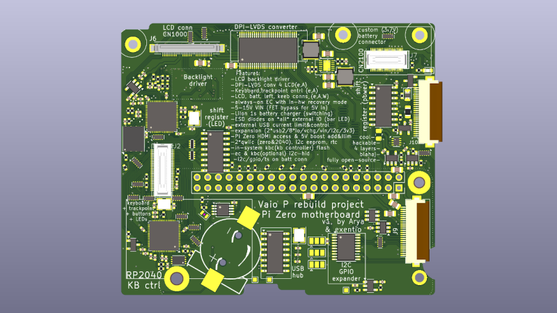
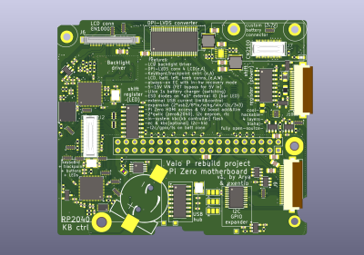 I recently finished and tested the first revision of this motherboard. It’s a tightly packed four-layer board, populated from both sides, and I want to show it off – describe how I designed it, the various low-level and high-level decisions that went into it, and strategies that I used to make sure this board became real and workable despite the odds.
First of all, the original article has helped in more than one way. Most importantly, I was lucky be contacted by [Exentio], a hacker who was also looking at remaking this particular Vaio with a Compute Module. He had designed two crucial blocks: a display parallel RGB to LVDS converter and a keyboard controller board. From my side, I could help and design review these boards, and design the backlight circuit, uhhh, eventually. Having these blocks was instrumental in me feeling comfortable enough to start the Vaio board design!
At some point in May, I realized I had the board outline and two of the crucial building blocks tested and ready to go, thanks to [Exentio]’s effort – there was barely anything else left that could hold me back. I started playing with the design by throwing these blocks into the schematic and copy-pasting some of my own general building blocks in, for instance, a PAM2306 dual-channel buck regulator, a USB hub, and two simple powerpaths for initial power management.
One trick that’s definitely helped from the start, is planning out locations for the building blocks using empty squares on the silkscreen, ensuring I’d keep space for everything. It didn’t have to be the perfect kind of planning, and I still had to move things here and there during layout, but it’s definitely helped in that I didn’t end up requiring any giant moves and rearrangements.
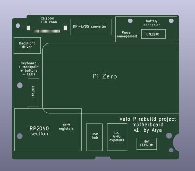
If you want to make your estimates more precise or make more educated layout guesses, don’t limit yourself to squares – just throw footprints (“Add Footprint”) onto the board before you even get to their schematic – any little bit of pre-planning that helps you avoid moving large chunks of your layout later. This applies doubly to connectors – you might not have the symbols for them wired up or even ready yet, but if you make sure the required external connectors are present on the board from the start, it will help you avoid some nasty moves.
Another crucial trick was spending about an hour-two on this board every day, for a week or two. A large project like this will take a fair bit of time, so you’ll want to make sure you can put tons of effort into it, and be emotionally prepared that it won’t happen in an evening’s time – this one took about two weeks. I also kept a TODO list in the schematic – you really want a place to note even the smallest things, from features, to potentially problematic spots that you’ll want to pay extra attention.
Space Constraints
When planning out a board with a large amount of passives, you want to make sure they’re as uniform as possible, so you have less to worry when ordering. In particular – what’s the size of passives you can afford in terms of board space? If you pick too large ones, you might run out of board space way way too quickly, becoming unable to route tracks
I standardized on 0402 components, which also meant I’d certainly be stenciling this board. It gets tiring to hand-solder parts given that this board has a thousand or two solder pads to touch. I opted to use 0805 for larger-value bulk capacitors for switching regulators and power rail purposes because 0402 10uF and 22uF capacitors get expensive if you want to get reliable ones, as we’ve discussed previously. In a few spots, though, I had to switch some 0805 capacitors to 0603, purely due to space constraints.
There are about a hundred resistors and a hundred capacitors on this board – remember, at some point, you can get a PCB fab to assemble just the passives for you, purely to spare yourself all the resistor and capacitor placement. You won’t get to stencil the ICs together with the passives, though, which is why I didn’t bother, because the RP2040 QFNs alone are annoying to handle without solder paste. Have you heard of Interactive HTML BOM for KiCAD? Make sure to use that, it’s simply wonderful and will prevent assembly errors of the kind that burn your board up before it’s even placed into the case.
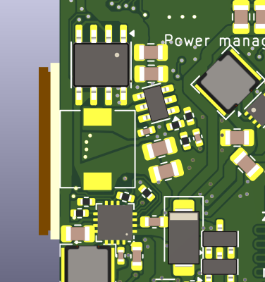
Inductors in the switching regulator can be an unexpected contribution to board space – if you need a 4.7 uH inductor and you need it to pass 5 A or more, take a look at online marketplaces before you even start designing the circuit, and see what the average size is for an inductor that fits your parameters. In my case, I got lucky, but only barely – some inductors definitely didn’t fit as well as I would’ve had hoped.
For this specific board, expected to fit inside the thin Sony Vaio’s shell, I had one more different thing to consider – component height. The original Vaio board was definitely designed in a way where all switching regulator components were placed on only one side, with plenty of height room for inductors and capacitors specifically. I placed all the switching regulators on one side, except one – the PAM2306 for the display 2.5 V and mod board extra 3.3 V rail.
In the end, I mis-estimated the inductor height, and had to shop for lower-profile inductors for that regulator. Thankfully, I found some decent lower-height inductors – they work wonders for powering the screen, and the only problem is that the inductor heats up more than I’d expect, but not too badly.
Source Considerations
Ordering the components for your board? Missing a position or two will really suck, and could delay your project by a week or two easily. My advice is to make sure that all component values are assigned and correct, and to pay the most attention to configuration and feedback resistors! Then, optimize the BOM, export the BOM out of the board into a .csv, and go through it line by line as you’re ordering. Alternatively, you can use the checkboxes in the InteractiveHTLMBoM – just that you’ll have to keep it open all throughout, a page refresh might have the checkboxes disappear.
When it comes to resistors, remember that you might have to improvise them on the spot – again, you don’t want to wait on them, so get a collection of resistor values. I bought a $15 book of 0402 resistors from Aliexpress, and it proved instrumental – especially given it lets you adjust values during bringup, and, it let me basically not worry at all about missing resistor values at all during sourcing. The earlier you order, the more likely will it be that one IC won’t go out – which has very much prevented me from testing out the display properly.
Apart from that, the book let me be a little more lazy and figure out switching regulator feedback circuits during assembly – and there’s nothing like being able to adjust your USB boost regulator to 5.25 V post-factum, or increasing backlight current in case you notice that the resistors you’ve calculated before result in a dim screen.
Hacks For Routability, Bootstrap, Motivation
This board’s switching regulators are probably worth their own article. There were two power hacks I ended up doing. The first one was having a separate always-on linear regulator for the EC, avoiding chicken-and-egg power problems. This one was certainly a success, and if you’re planning a motherboard that will also have to go low-power at times, you might really want a separate regulator for your EC.
The second one was making use of the Pi Zero’s 3.3 V regulator for powering a ton of stuff, like the keyboard controller chip, the LVDS transmitter, the USB hub, and – basically, everything that would only need to run once the Pi would be powered. This constrains the Zero’s onboard 3.3 V regulator, sure, but it’s not too much of a problem – I’ve powered tons of stuff from the Pi Zero’s 3.3 V rail in the past. It also has helped quite a bit, because the less switching regulators I have to design and keep track of, the better.
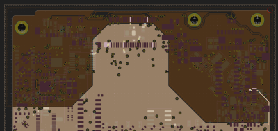
A big problem was making use of board layers correctly. I went for four layers on this board, with one 3.3 V layer which carries the output 3.3V rail from the Pi Zero, and one GND layer: SIG-GND-PWR-SIG. Later on, I took a look at the 3.3 V polygon, and realized that nothing used 3.3 V on a big chunk of the board. I deliberated some, and added an extra GND polygon covering a good third of the 3.3 V layer on the path where all the switching regulators were concentrated, and specifically, the path where the DC input jack current would flow into the switching regulator providing 5 V. It’s a plane split, sure, which is not great as far as signal return currents go, but there was one continuous GND layer right next to it already. Fingers crossed it works out for me long-term!
I kept inner layers as clean as possible generally – however, some tracks still had to go on inner layers. My compromise for having good inner polygons was keeping the inner layer traces as close as possible to the edge of the board, ensuring that there’s the least amount of plane splitting possible.
The cherry on top of the cake? I used the KiCad board image generation hook for GitHub that I covered this year, and, it’s added a surprising source of motivation to the project. Each time I’d push changes to the repository after a day of board design work, the board image would regenerate, showing off my changes – a lovely conclusion to my work and a reminder that I’ve done well with it. Also, I could demonstrate the board additions to my friends, including [Exentio] – can’t deny, having a social element to this design has really helped in getting this board completed!
There are a few fundamental aspects left – like power management, making plans for board assembly and bringup before you send off the board to manufacturing, and giving yourself the best chances for success when assembly and bringup time comes. That’s within a week – together with a report on how the board is working out so far!





Remind me again: what kind of Vaio? Sony named just about everything that could run programs a Vaio for a few years there. Are we talking a PocketPC or a Laptop?
I thought I remembered it being the laptop from a previous, related article. After looking a bit more, I see it’s tagged with “laptop hacks”.
The Vaio P series, a tiny pocketable computer – I show a pics of its outsides and insides in the previous article! Not your average Vaio device for sure – this one’s a collector’s piece of sorts. It’s also damn good hardware-wise, as far as the form-factor/keyboard/display go!
Great project, I love the look of the Vaio P series. Well worth the work bringing it useable in this age, although if it were me I’d probably try designing it around a Compute Module 4 or even now a CM5.
This is fantastic, I would kill for a small palmtop computer that I could run Ubuntu on at a modern pace. IMO a Pi 5 computer module would be way more useful than a Pi Zero.
GPD make some nice ones. You wouldn’t write your thesis on any of the keyboards, but they’re good enough and the computer still fits in a (large) pocket. I’m using the GPD MicroPC, partly because it’s one of their cheapest, partly because it’s tough, partly for the awesome physical ports – proper ethernet, DE9 serial port and USB-A ports. Mine’s running Linux Mint, and everything works.
i used to really lust after the tinier laptops, like 25 years ago. it took a long time for ‘ultrabook’ to live up to its promise but finally now the bargain-basement 12″ laptop is fantastic. tiny, light, fantastic battery life, gobs of RAM and CPU and storage, suspend-on-lid, integrated wifi&bluetooth, high-speed USB, just everything i ever wanted. it’d be very hard to compete with the kind of 12″ laptop you can buy new for $200 these days. there are even smaller laptops if you really want it (but imo tablets and cellphones make more sense at those smaller sizes).
so the only reason to build something like this is if you’ll never use it. :( if you’re building for use, i just can’t imagine bothering with the downsides
Same.. Although I never really grew out of it.
I used an eeepc701 for years until the hardware became a bottleneck (Only 4GB of internal storage makes things tough now). Same with an OpenPandora UMPC.
Nowadays I have a plethora of Samsung Chromebook 3’s. They are EOL, but only run about $35 and linux works like a charm on them. I know most people would poo-poo the specs but it is good enough for most stuff, the battery lasts a long time, 11.6 in in size, cheap enough that I don’t care about it, and for compiling I still have my beefy desktop.
Good choice for a throw around laptop that you don’t worry about.
Fast enough SSD, easy to use and lightweight desktop environment, and you’re laughing. I picked up a Lenovo T440 for peanuts from a charity shop, upgraded to 8gb ddr3, and a 256gb m.2 sata in a sata converter and updated to coreboot, it’s become my main Linux box for on the road.
i finally bricked my last ARM chromebook, and i’m sad to admit i just don’t care enough to revive it :(
(but only because i have a $200 “PC” that took its place)
Very interested in this project. I got a spare shell and screen with the intent to do this one day myself, but absolutely got stuck on the screen part. It’s exciting to know someone has already figured out the screen and the keyboard!
Will you be selling this board at all? And (aside from space) is there a reason you went for a pi zero rather than. A compute module for a pi 4/5?
Oh and last question, can you change out the stock battery with something nicer here
I used an eeePC for a while (the 9 inch one for me) but what killed it for me was the battery that drained in a week even if the thing was fully shut down. In 2021 I bought a “MicroPC” from GPD and am thrilled with it. 7 inch screen and lots of ports: USB, microSD, proper ethernet and even a DE9 serial port! It has 8GB of ram and Linux Mint works like a dream. If you have big pockets (like cargo pants) it fits in your pocket and will run for most of the day under intermittent use. It charges from USB-C, but even a crappy old phone charger will (slowly) do that job at 5V, 500mA.
Arya, where can I find your repository for this project? I searched your GitHub but failed miserably in locating it. Want to upgrade one of my Vaio Ps, super keen to follow on your footsteps.
It’s in https://github.com/CRImier/MyKiCad/tree/master/Reverse-engineering/sony_vaio_p_re
Nice, thanks a bunch!!!
thank you for posting it before I got to it!
No worries, love this project and I am keen to use it to make my Vaio P useful again, when I have time.
ow sorry for that, somehow I forgot to include that link into the article! included now, and, here’s my monorepo page on it
Raspberry Pi anything is completely ill suited for DIY laptop/cyberdeck projects because it does not support suspend to ram a feature laptops have had for multiple decades now.
If you are done using it, shut it down.
If you aren’t done using it, then use it.
Suspend to RAM encourages bad behavior.
Even when new Vaio’s needed reviving. They usually looked cool but managed to make overpriced, painfully under powered machines, choked even more by bloatware. I wanted a Vaio until I actually used one. Subsequent iterations and form factors over the years have not changed my opinion of them. I’m sure this rebuild, blows anything Sony ever produced, out of the water.
Great project! One question: What does EC refer to in “always-on linear regulator for the EC”?
And do you need under-volt protection for the battery before that linear regulator?
possibly “embedded controller”
handles various hardware in a laptop (e.g. keyboard, pointing device, power button, indicator lights and backlights, general miscellaneous stuff)
Have you not considered using a pi compute module instead of a zero?
Hello! I have one and I’ve already thought about doing something exactly like this, however, I thought about designing a motherboard like the original only replacing the components with newer ones, I don’t know if it’s possible to design and ask some factory to run… Excited by your progress. Accompanying from here. Brazilian greetings