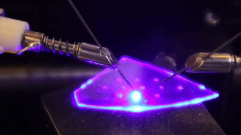
An irregular shard of a crystal wafer is set on a table, with two wire probes contacting it. Between the probes, a bright blue-purple light glows, illuminating the rest of the wafer.

Making LEDs In The Home Fab

Impressive as it most certainly is when an amateur fabricates a semiconductor, most of the projects we’ve seen are more demonstrations than workable chips. [Dr. Semiconductor], however, is going much further with his fabrication process, and is already working on a method to bond chips to printed circuit boards. It’s difficult to align a PCB with the pads on the underside of an opaque silicon wafer, however, so as a trial run he’s made and bonded some transparent LED chips.

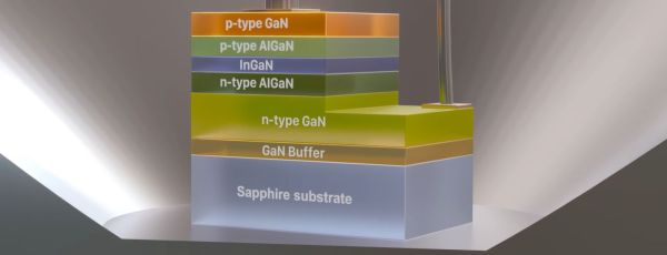
The starting material for these chips is a gallium nitride (GaN) LED epiwafer, a stacked structure of n-doped GaN, an indium gallium nitride quantum well layer, and p-doped GaN grown on a sapphire substrate. When current passes through the structure, electrons from the n-doped layer and holes from the p-type layer recombine in the quantum well layer, emitting blue light. To make a functional LED from this, [Dr. Semiconductor] needed to make electrical contacts to both the n-type and p-type layers. Making the n-type contact required cutting through the p-type and quantum well layers.

This would normally be done with reactive ion etching in chlorine, but [Dr. Semiconductor] came up with a new process: a 355-nm ultraviolet etching laser causes GaN to break down into gallium and nitrogen, with the resulting cut being cleaned up by a potassium hydroxide etch. To deposit the contacts themselves, [Dr. Semiconductor] formed a photoresist mask, deposited metal (nickel, silver, and titanium) in a sputtering chamber, and used a developer solution to dissolve the mask and lift off the unwanted metal regions.
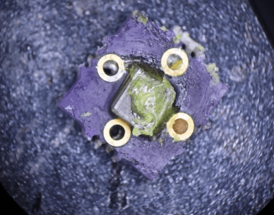
A square, purple PCB is shown under a microscope. The PCB has four vias surrounding a transparent chip, which has a blob of translucent yellow material on top of it.
The LED after bonding and phosphor application.

When [Dr. Semiconductor] applied current between the two contacts, the LED glowed bright blue. The next step was to mount it to a PCB; to do so, he first sliced the wafer into individual LED chips with the ultraviolet laser. He then electroplated indium bumps onto a printed circuit board, positioned the chip above these bumps, added some rosin flux, and melted the indium bumps. This soldered the chip to the board and let the board power the LED.

Like most commercial LEDs, these were blue; most LED assemblies additionally include a phosphor layer which absorbs blue light and emits another color. To create a white LED, for example, [Dr. Semiconductor] mixed cerium-doped yttrium aluminium garnet phosphor powder with clear silicone and spread it over the LED. This absorbs some of the blue light and emits yellow light, and the resulting mixture of blue and yellow light looks white to human eyes.

We’ve previously covered some of the history of LEDs and the phosphors which make them useful. This seems to be the first inorganic LED we’ve seen, but we’ve also seen a few homemade OLEDs.

Thanks to [SpuriousIndices] for the tip!
Shuji Nakamura: The Man Who Gave Us The Blue LED Despite All Odds

With the invention of the first LED featuring a red color, it seemed only a matter of time before LEDs would appear with other colors. Indeed, soon green and other colors joined the LED revolution, but not blue. Although some dim prototypes existed, none of them were practical enough to be considered for commercialization. The subject of a recent [Veritasium] video, the core of the problem was that finding a material with the right bandgap and other desirable properties remained elusive. It was in this situation that at the tail end of the 1980s a young engineer at Nichia in Japan found himself pursuing a solution to this conundrum.

Although Nichia was struggling at the time due to the competition in the semiconductor market, its president was not afraid to take a gamble on a promise, which is why this young engineer – [Shuji Nakamura] – got permission to try his wits at the problem. This included a year long study trip to Florida to learn the ins and outs of a new technology called metalorganic chemical vapor deposition (MOCVD, also metalorganic vapor-phase epitaxy). Once back in Japan, he got access to a new MOCVD machine at Nichia, which he quickly got around to heavily modifying into the now well-known two-flow reactor version which improves the yield.

Continue reading “Shuji Nakamura: The Man Who Gave Us The Blue LED Despite All Odds”

We Ruined Status LEDs; Here’s Why That Needs To Change

Ah, the humble status LED. Just about every piece of home electronics, every circuit module, and anything else that draws current seems to have one. In the days of yore, a humble indicator gave a subtle glow from behind a panel, and this was fine. Then the 1990s happened, and everything got much much worse.

It’s Not The Technology, It’s How You Use It

With great brightness, comes great responsibility.

The 1990s brought us much good: Nirvana, Linux, and of course the blue LED. Much like “Teen Spirit”, the latter quickly fell into overuse: the technology rapidly became the sigil of all that was new and great, much to the ocular pain of the buying public.

This decision ranks up there for stupidity with other such questionable choices as hiring a rental car at the airport, or invading Russia in the winter. A status LED, most would agree, is there to indicate status. It need only deliver enough light to be seen when observed by a querying eye. What it need not do is glow with the intensity of a dying star, or illuminate an entire room for that matter. But, in the desperate attempts of product designers to appear on the cutting edge, the new, brighter LED triumphed over all in these applications. Continue reading “We Ruined Status LEDs; Here’s Why That Needs To Change”