The Gerber Behind Gerber Files

When we create a printed circuit board, the chances are these days that we’ll export it through our CAD package’s CAM tool, and send the resulting files to an inexpensive PCB fabrication house. A marvel of the modern age, bringing together computerised manufacturing, the Internet, and globalised trade to do something that would have been impossible only a few years ago without significant expenditure.

Those files we send off to China or wherever our boards are produced are called Gerber files. It’s a word that has become part of the currency of our art, “I’ll send them the Gerbers” trips off the tongue without our considering the word’s origin.

This morning we’re indebted to [drudrudru] for sending us a link to an EDN article that lifts the lid on who Gerber files are named for. [H. Joseph Gerber] was a prolific inventor whose work laid the ground for the CNC machines that provide us as hackers and makers with so many of the tools we take for granted. Just think: without his work we might not have our CNC routers, 3D printers, vinyl cutters and much more, and as for PCBs, we’d still be fiddling about with crêpe paper tape and acetate.

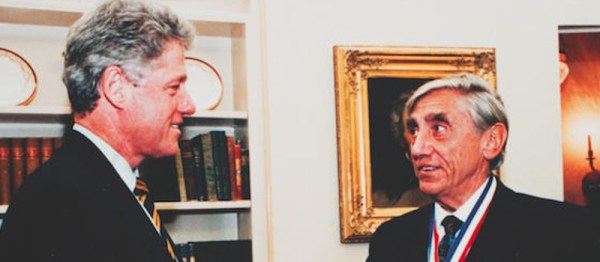
An Austrian Holocaust survivor who escaped to the USA in 1940, [Gerber] began his business with an elastic variable scale for performing numerical conversions that he patented while still an engineering student. The story goes that he used the elastic cord from his pyjamas to create the prototype. This was followed by an ever-more-sophisticated range of drafting, plotting, and digitizing tools, which led naturally into the then-emerging CNC field. It is probably safe to say that in the succeeding decades there has not been an area of manufacturing that has not been touched by his work.

So take a look at the article, read [Gerber]’s company history page, his Wikipedia page, raise a toast to the memory of a great engineer, and never, ever, spell “Gerber file” with a lower-case G.

Recreate A PCB With A Scanner And Inkscape

turnsig

[John] has managed to replace a broken turn signal PCB by scanning it and converting to Gerber format. [John] purchased a Triumph Spitfire with toggle switch wired up for turn signal control. The “official” replacement part worked better than the toggle switch, but it didn’t cancel after turning. He was able to get the original switch, only to find it had a hole completely burned through the phenolic board. This isn’t completely surprising, as Triumph used a Lucas Industries electrical system. As anyone who has owned a car with a Lucas “prince of darkness” electrical system will tell you, Lucas systems were not known for quality. A quick Google search brings up plenty of pages attesting to this.

Phenolic resin/paper was a common early PCB material.  The FR-4 fiberglass boards most commonly used today could be considered descendants of FR-1 and FR-2 phenolic. (The FR in this case stands for Fiber Reinforced). The standardization worked in [John’s] favor, as his burned board was 31 mils thick, which is still a standard PCB thickness. Re-creating an odd sized board such as this isn’t a hard job. It would however mean spending quite a bit of time with a ruler and a caliper. Rather than spend all that time measuring and re-drawing, [John] scanned his PCB on a flatbed scanner. He used graph paper as a background to verify the image wasn’t being stretched or skewed.

[John] brought his scan into inkscape, and traced both the outline and copper areas. The outline and copper had to be exported as two separate files, so he added corner marks outside the board outline as fiducials.  He then used pstoedit to convert inkscape’s eps output files to gEDA pcb format. The two files were rejoined in gEDA. From there [John] exported a Gerber, and ran it on his home PCB milling machine.  The results look good. [John] plans to make another revision of the board from a professional PCB house with vias to hold the copper to the substrate.