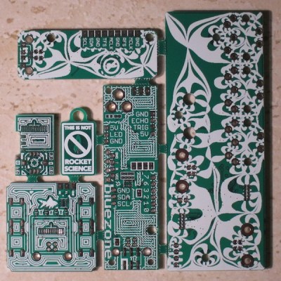
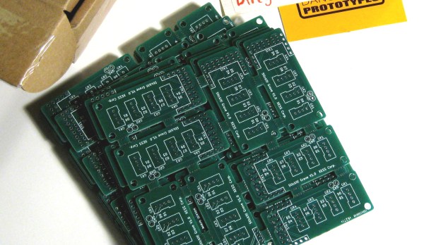
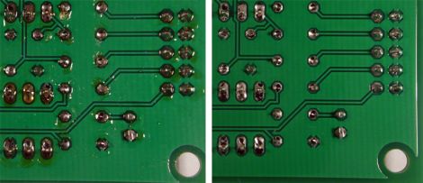
Anyone who’s made a PCB has encountered the conundrum of having to pay for space that you don’t use… for instance, designing a round PCB and seeing the corners go to waste. The solution? Smaller boards added to the blank spots.
One logical stumbling block might be that you simply don’t have a small PCB design ready to go. Latvian hacker [Arsenijs] created a resource of small PCBs that can be dropped into those blank spots, as well as a tutorial on how to combine the gerbers into a single panel.
 Great minds think alike, and this guide is following hot on the heels of [Brian Benchoff’s] article on panelization. They’re both a great read. It’s interesting to think that not long ago we would see multiple guides on home etching boards and now we’ve climbed the production ladder to guides that help better utilize PCB fab houses. Neat!
This project seems a logical spinoff of [Arsenijs]’s ZeroPhone Pi smartphone project, a finalist for the 2017 Hackaday Prize that makes a low-cost phone using a stack of PCBs. One imagines that while prototyping the phone [Arsenijs] ended up with a lot of wasted space! Fill that up with smaller designs like breakouts, or decorative items like a hackerspace business card. If you’re looking for small PCBs you can find a few in the files area of the project on Hackaday.io. Otherwise, you can share yours and [Arsenijs] will add them.


