Die of an Altera EPM7032 EEPROM-based Complex Programmable Logic Device (CPLD). (Credit: ZeptoBars, Wikipedia)

Using EPROMS And EEPROMs As Programmable Logic With Lisp

That EPROMs, EEPROMs and kin can be used as programmable logic should probably not come as a major surprise, but [Jimmy] has created a Lisp-based project that makes using these chips as a logic array very straightforward. All it takes is importing the package into one’s Lisp project and defining the logic, before the truth function generates the binary file that can be written to the target chip.

Suggested is the one-time-programmable AT27C512R EPROM (64k x8), but any 8-bit parallel interface (E)EPROM should work, with non-OTP chips being nice unless the chip has to go into a production device. A possible future improvement is the addition of 16-bit (E)EPROM support.

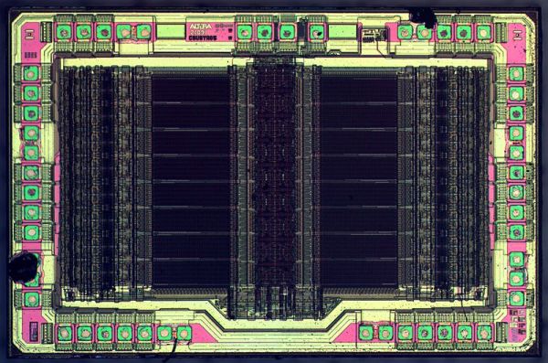
The use of EEPROMs is common with PLA-replacements, as with, for example, the Commodore 64, where the official PLA IC tends to go bad over time. Due to the complexity of the logic in these PLA ICs, here CPLDs are used, which internally are still EEPROM-based, but feature many more programmable elements to allow for more complex logic. If all you need is a bit of glue logic and you are looking for something in between a stack of 74-logic ICs and a CPLD, an EEPROM may be just be the solution, regardless of whether you prefer to create the binary image with Lisp or C.

Continue reading “Using EPROMS And EEPROMs As Programmable Logic With Lisp”

Die Photos Reveal Logic From Commodore 128 PLA Chip

The 8721 PLA, or programmable logic array, was one of the chips that had to be invented to make the Commodore 128, the last of the 8-bit computers that formed the leading edge of the early PC revolution, a reality. [Johan Grip] got a hold of one of these chips and decided to reverse engineer it, to see what the C-128 designers had in mind back in mid-1980s.

PLAs were the FPGAs of the day, with arrays of AND gates and OR gates that could be connected into complex logic circuits. [Johan]’s investigation started with liberating the 8721 die from its package, for which he used the quick and easy method favored by [CuriousMarc]. The next step was tooling up, as the microscope he was using proved insufficient to the task. Even with a better microscope in hand, [Johan] still found the need to tweak it, adding one of the new high-quality Raspberry Pi cameras and motorizing the stage with some stepper motors and a CNC controller board.

With optics sorted out, he was able to identify all the pads on the die and to find the main gate array areas. Zooming in a little further, he was able to see the connections between the matrices of the AND and OR gates, which makes decoding the logic a relative snap, although the presence of what appears to be an output block with latching functions confounds this somewhat.

The end result is a full Verilog HDL file that reflects the original 8721 logic, which we think is a pretty neat trick. And we’d love it if our own [Bil Herd] could chime in on this; after all, he literally designed the C-128.