
There is a wide assortment of cheap development (dev) boards for Complex Programmable Logic Devices (CPLD), the smaller cousin of the Field Programmable Logic Array (FPLA)
Using an inexpensive board and the development software that’s free to download from the major programmable companies such as Xilinx and Altera, the only additional thing needed is a programmer module. Cheap ones are available on Ebay but I am hoping that someone takes the time to teach an ARM/Arduino to step in as a programmer.
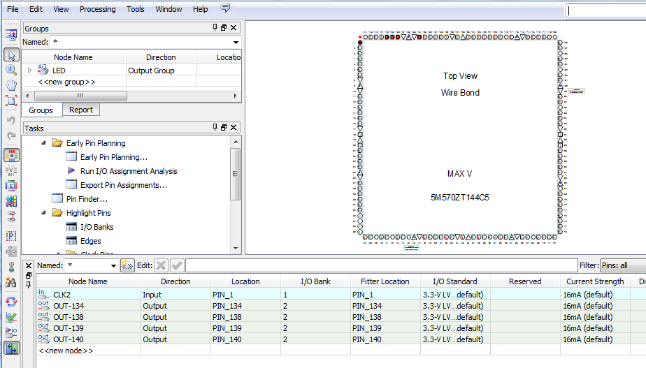
I have a small collection of dev boards including some Ebay specials and also designs I did a few years ago to choose from. For today I am grabbing a newer board that has not been fully checked out yet; an Altera Max V device. I have stuffed the CPLD, the clock oscillator, some LED’s and part of the onboard power supply along with the JTAG header needed to program the CPLD and that’s about it.
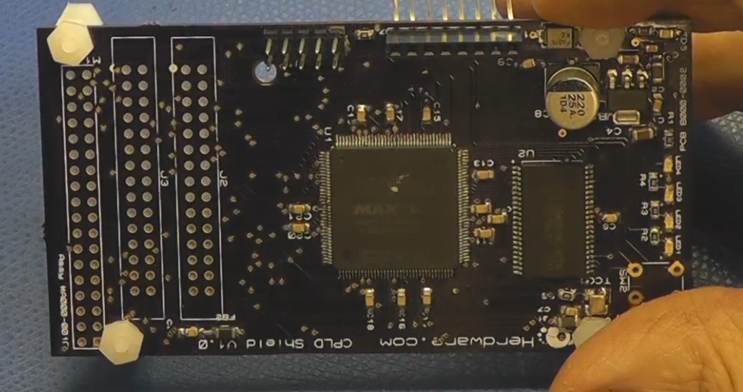
On the outside the important signals are a master clock (NOTHING happens without a clock) and then there are the LED outputs that let us know something is going on. In the old TTL days you usually couldn’t drive an LED directly, so that ability in itself is a sign of the times.
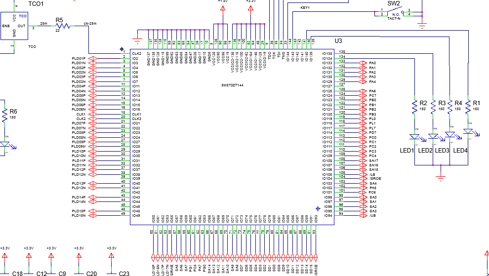
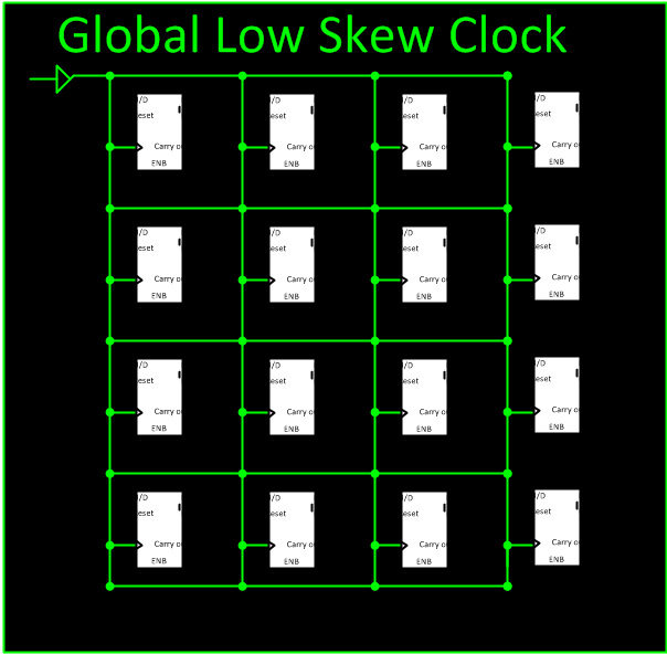
Starting with the clock input you can see the pin and oscillator below. We will use settable parameters in the software to wire this input to the low-skew global clock (gclk) distribution network. The difference between when the clock arrives at the various register across the entire device is known as skew and if it is noticeably late or early to some blocks it could have a drastic effect on the logic. (latches old or intermediate data when everything else latches the current data.
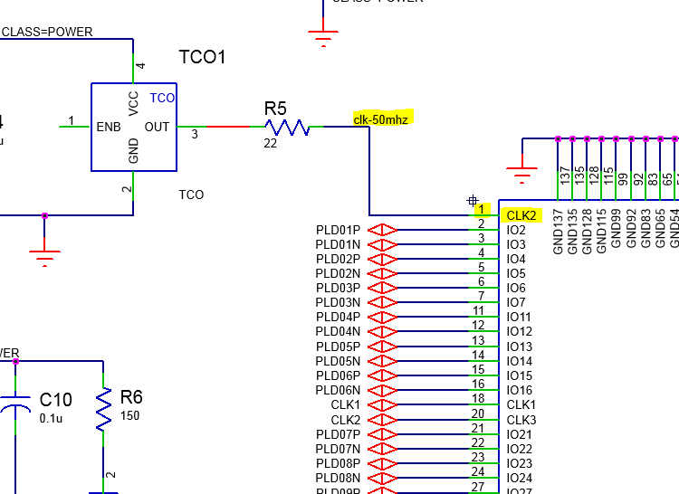
The 22 Ohm resistor in the clock flow is placed near the oscillator and matched impedance and absorbs reflections, but more on that in a different video.
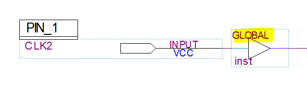
Once the clock makes it into the device we need to get it connected to the global clock. This is accomplished at a schematic level, and I chose to use a schematic on the top level, by adding a primitive marked Global. If using an HDL language you would specify a global primitive as well.
Once connected to the global clock, there are also auxiliary clocks and “regional” clocks for different zones, which look like this:
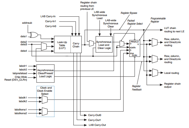
The drawing above is an over simplification, one of the Altera Max logic blocks actually looks like the diagram below.
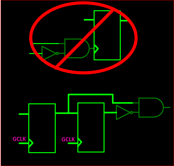
A very important concept while living on a chip is that it is unsafe to try to predict a minimum delay and that gates in nearby silicon are so fast the simple logic may propagate glitches or unknowns. All of these issues affect the suitability of using combination logic to drive a clock input. A good technique is to do a fair amount of computational calculation and then stop to save the results in a register with a global clock, a technique referred to as pipe-lining
An example of reverting back to clock driven may look something like this for detecting a rising edge.
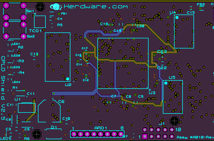
At some point we need to interface to the outside world. In a heavy utilization design the PCB layout waits until the programmable logic is significantly done, at least enough that it would still be compileable even with the pin assignments permanently frozen (the compiler loves to pick its own pins). In my case I froze the pins already when I designed the PCB and assignments can be seen here.
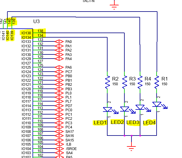
I named the pins to reflect the pin number that matches the PCB and so I can easily connect up the pins from the inside.
As I mentioned I like to have a schematic as the top sheet of the design and I do any sizing or inversions there as it is more intuitive for a dinosaur like me. Our design will look like this when completed with a 64 bit counter dividing down the 50Mhz clock to something visible.
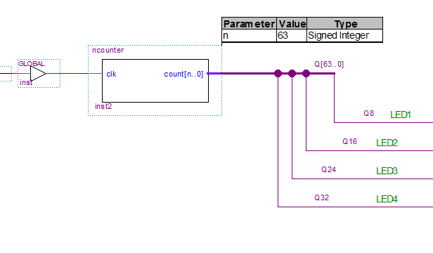 We have yet to define the counter, which I call ncounter as I will make it n bits large depending on a parameter I set. Using an editor and the nine fingers left to me I created this overly simple file. I say overly simple as I didn’t include reset and other housekeeping logic that helps both the physical and the simulation results (I say nine fingers because I tore one-off last summer).
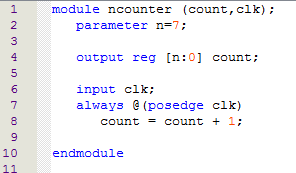
Once typed and saved a click causes the “Create Symbol” command is run and the ncounter symbol is created. The parameter that sets the width defaults to 7 (8 bits) but is overridden with 64 bits pushed down from the top sheet.
Finally I show a little of how I dealt with the fact that the Max V device has a core voltage of 1.8v and I have elected to run the interface pins at 3.3V making this a dual voltage part. I use Proteus by Labcenter for schematic and PCB ($248USD) and one of its strengths is that it has a powerful auto-router that routes faster and better than I ever could. I don’t hand route as inevitably there will be changes and the time spent re-hand-routing is time I don’t have. So essentially I teach (constrain) the auto router how to do better each successive pass.
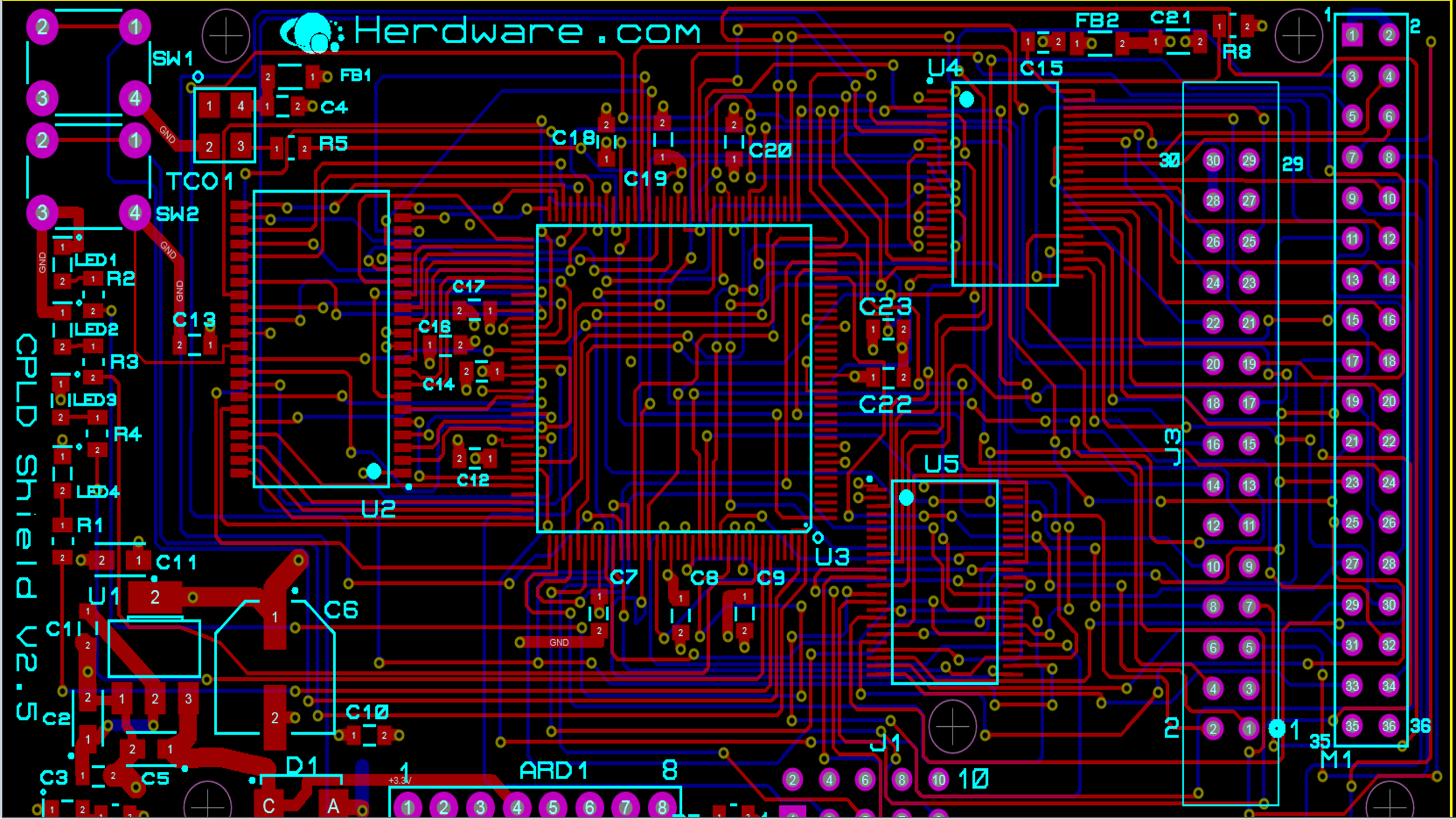
This is a 4 layer board with ground as the 2nd layer (from top) and +3.3V as the third layer since it was used by the peripheral chips as well. That left the need for routing the core 1.8V supply for the CPLD.
As shown below I created a loop shaped supply path for the 1.8V supply with a couple of internal interconnects on the two inside layers. I jump layers often so that ground return (and +3.3) current can follow straight paths to the sources and not have to go around to find an exit path. Also the center maintains a lower impedance rather than being isolated by being surrounded on almost 4 sides.Having a loop reduces both DC and AC resistance as not only is there parallel paths at work, there is no stub for things to reflect off of. Stubs are typically bad.
Using the programmer built into the software I upload the code after I compile it and the LEDs blink. You don’t have to take my word, you can watch the video… I promise there is very little CGI at work.
While this is just the briefest of run-throughs, if you followed along you have experienced all of the steps to program a CPLD or even an FPGA.
I am thinking about taking the version of this PCB that not only has the fast SRAM but also voltage level converters to allow the interface to voltages like 5v. One thought is to make an Arduino driven logic analyzer since the Arduino doesn’t need to run “at speed” — the CPLD hardware takes care of all of that.


OMG shorten this post on the front page!
Done. Thanks for the heads up strevo.
Good lookin’ out, both of you.
Check out the Guzunty for the Raspberry Pi – that solves the programmer problem.
Hackaday – Keep the Bil Herd stuff coming, please.
Bil, you remind me of some of my best mentors! They knew so much you could just feel it, and it was often a race up a learning curve (at first) in order to acquire the base understanding necessary to really appreciate and absorb all the knowledge they were sharing.
Constructive feedback: have someone edit your write-up a bit more, and do not forget the golden rule of writing: to tell us all what you are going to show us, then show us, and then tell us all what you have just shown us.
Bil Herd = Gravitas.
Agreed, pleasurable reading. Stuff like this keeps me coming back hackaday…
Makes me want to blow the dust off my Papillio one and actually do something with it. Maybe emulate a vic20.
Why would you want to emulate a VIC-20 on a FPGA when it can be done on a standalone Arduino-Uno with NTSC video?
http://www.hackster.io/janost/the-nano-vic-20
Go for something much better if you have access to a FPGA.
Well, nice project, but only monochrome and it doesn’t support all features of the VIC chip, for which you need a very fast microcontroller (the Atmega chips are really slow compared to a fast STM32 ARM chip with 168 MHz), or a FPGA. With a FPGA it is even easier to implement it, and it is fun, too :-)
I count on Mr. Buss to keep me in line, he has already pointed out that I completely missed the fact that two “similar” Arduinoish boards where two different voltages on one project we were looking at. ( I assumed that you would not use the same footprint for incompatible and variable designs or voltage. It would be great if they would print the voltage so you don’t have to look up that particular board)
It didn’t make it through editing but Frank and I are looking at the spin-off of this board as an open source logic analyzer..
Glad I can help you, Bil, even if it is only a second pair of eyes and stating some obvious things, because you know much more about electronics than I do. Always interesting to read your articles and watch your videos.
As I wrote in the last eMail, I’m prototyping the logic analyzer on my Parallella board (for analyzing my C64 MIDI cartridge). Coding gets easy if you have a really big FPGA with many LUTs and hundreds of kb block RAM, connected in the same chip to a dual core ARM CPU with a 100 MHz / 32 bit memory mapped data bus, and HDMI output. I can even implement muxes for each of the 32 bits I plan to record to map they individually to one of the 48 GPIO inputs and the FPGA is still not half full :-) But it should be possible to implement some ideas for the CPLD as well, like a control register which starts the sampling, and a counter with which you can specify how many samples are sampled until it stops after a trigger condition was met, to move the trigger point to whatever position you want, and some registers and logic for falling/rising/bit-pattern/mask-trigger etc.
Why would you emulate a VIC 20? Because if you emulate a Cray-1A you cant find any software for it!
http://www.chrisfenton.com/homebrew-cray-1a/
Fortran version of “Adventure”? (Colossal Case)
You’re in a maze of twisty passages, all alike.
IIRC the Bus Pirate can do JTAG for CPLD programming. It’s not fast, but you won’t need to buy another board.
https://www.kickstarter.com/projects/13588168/papilio-duo-drag-and-drop-fpga-circuit-lab-for-mak#
Give me fewer Arduino, 3D printer, and quadcopter articles, and replace them with more Bil Herd content.
mooltipass posts as well?
+1
and BTW great article series, thanks Bil & HaD
Ok, you opened the door, what’s the story that goes behind the statement “I tore it off last summer”? I’m always curious about such things, I’ve got plenty of scars myself.
I am curious to.
I had the two little fingers on my right hand broken beyond use. It was a total pain as I am a coder and all the extra keys for coding are under those two fingers.
I moved my left hand across one key and my right hand across two keys so that I type with the five fingers of my left hand and the three on my right. It took me six months to get used to. I am not as fast but I do ok.
ITS HARDWARE NOT HERD … oh wait now i get it -u-
Arduino can do the same thing, it will be slower but it’s also so much easier for those who don’t like programming.
Not so sure about the 1.8V routing. It is the lowest voltage so there is less margin for it to drop before it goes out of specs than your 3.3V. I would assign a much higher priority than the 3.3V. Those thin tracks that are not even cleaned up and minimized for length…
I would create a 1.8V island inside, followed by an outside ring of thick track for the 3.3V I/O (still inside the peripheral of the chip). There is a school of thought that the plane capacitance would do some good for the core voltage at high frequency. As long as the 1.8V is well decoupled inside the island, then you can get away running a *thick* track to connect it to rest of the board.
BTW The 2nd picture has be cropped on the right hand side and the X direction is stretched on my browser.
I’ve been told you want to be careful with loops and use them wisely. Eg ground loops that cause problems with radios, speakers or poorly designed USB devices. However they work well in say.. low speed button arrays in order to increase reliability in case part of the loop breaks.
Now… I’ve seen where PCBs have loops around the outside of the board or IC. This is to suppress outside interference? Like a built in RF shield?
But if you do that on your V traces instead of the ground aren’t you introducing unnecessary noise into the circuit? In other words, wouldn’t your 3.3V ring (and the 1.8V ring in the article) pick up unwanted noise?
That loop around the outside of the board is called a “guard ring” and is exactly for what you describe. Being the loop in the same plane than the “radiators” effectively shileds them. Also works the other way around to shield sensitive inputs from the rest of the layout.
Also, as others have pointed out, I’m not sure if these 1.8V loops may cause EMI trouble because the size seems just right to resonate at a few hundreds of Mhz laying around fast switching signals.
But being Bil for sure he must know. Didn’t you hear the story of the early days about the jumper cable that saved the c64 pcb layout? He should tell!
You can tell in the TED series of computers when I took over the design as the guard ring appeared. We figured up a spacing for via’s to bond top to bottom guard rings so as to try and eliminate small dipole or antennas that may exist (even bad ones add up). The right site piece of metal can act like an antenna at certain frequencies and then they become energized by nearby EMI. The nearby EMI doesn’t need to be of the same frequency to impart some of it’s energy, and you end up with a re-radiator. The area around an aperture can pick up a dipole as well.
So the vias in the guard ring were to make sure eddy currents didn’t build or some kind of funny resonant sandwich develop. If you have seen a ground plane broken into a grid we did that in the old days to save metal (assuming its reclaimed) but also to break up eddy currents. With that said I am an old burnt out engineer and the new knowledge may be that eddies weren’t a problem. Also the new knowledge is not to hyperventilate a head trauma pt in an effort to reduce ICP so go figure.
The key with any shielding like a guard ring is that it should not be current conducting, Often a shielded cable will only ground at one end for this reason. Without current you cant have an inductive field, no field, no EMI.
Can say much for the historical side, but as far as I know ground mesh (instead of solid) and sometimes isolated copper patterns on routing layers (i.e. non plane layers) are used for copper balancing and to prevent board warp-age these days. Meshes also have better adhesion, but I don’t think that is the prime reason.
As for ground stitching around PCB is to act as a Faraday cage to prevent effects of the fringe field edge radiation (i.e. internal layers leaking out EMI that is radiated from the edge.) That’s also the reason why the internal layers and power planes are receded. (the “20H rule”) The vias forms a slotted aperture and their spacing control how high a frequency you want to block – sort of like a 1D version of the metal mesh in a microwave door blocking off the microwave and still let you peek inside.
emcmadesimple.com/pdfs/publications/PCB_Edge_Termination.pdf This talks about the fringing effect even though it is a paper that tries to avoid the 20H rule by doing terminations.
I am known for pointing to the screen in a microwave oven and babbling about Plank’s Constant. My son is known for rolling his eyes and getting away with his heated mac and cheese as fast as possible.
The warpage issue is cool. At some point in big quantity production the production engineers start getting involved and they take your carefully nurtured project and start changing things.for issues like warpage or metal recovery or flaking soldermask. I have usually been able to blur that hand-off by inviting the production engineers to critique the design sooner and in return they teach me what and why they do what they do. Heh, I learned Japanese in the 80’s specifically to have a better rapport with the people who where going to take my child away from me.
First off, this is not audio stuff which can amplify a few mV worth of signal very easily.
You are also dealing with a solid ground plane that have low impedance between all the connections to it across the PCB. Given that (singled ended) digital signals are all referenced to ground, you would want to have as solid a ground as possible. Why would you want to cut that up?
If you have very good decoupling for the I/O rail ring *to ground*, your I/O and core voltage rails would have a very low impedance to ground and that’s all that matters. This means that they are less susceptible to injected noise current from your circuit or outside sources (than a poorly decoupled ones).
“Having a loop reduces both DC and AC resistance as not only is there parallel paths at work, there is no stub for things to reflect off of.”
I am not sure if the author understand the concept correctly… If you have done your decoupling properly, you would minimize high frequency *AC* component in your voltage rail (i.e. they are close to DC). No AC components means there won’t be reflections!
“Stubs” which would be an incorrect term in this context, but you would want to minimize “trace inductance” (which is a better term) of your power rails which translates to (AC) impedance. But the way it is done in the layout is really really bad.
There are times where the power rail gets noise induced on it that resemble signal propagation just as signals get noise induce through capacitive and inductive coupling as well as shared IR.
I have seen a power rail that rang like a bell when devices were activated and so I mixed my metaphore a bit as I have 8 minutes to spit out a whole bunch of stuff and hope I don’t drastically mis-speak in the process. .
The layout is fine for what I need it for and the amount of time I put in to it. For a serious product I would have the design parameters dictate the layers and decoupling strategy and I would do an impedance analysis of all critical signals.
However thats the opposite of what I was actually trying to say is you don’t need to know all of that to just get started and to have fun.
While I agree with you on what I would do regarding the 1.8V, you’re still talking about something like a 15-20 mil track. On 1 oz copper that’s like, 20 mohm/in, so you’re talking about at most, 0.1 ohm. Even if it pulls an amp (which it can’t), that would still only be 0.1V drop. The bigger concern, of course, is the loss of the plane capacitance. For a (slow) CPLD this isn’t going to be a big deal, but for an FPGA plane capacitance takes over in the ~few hundred MHz or so, so it’s a real effect.
Of course the *big* concern you didn’t mention is that he routed that *on both interior layers*. One of which is ground.
Except for very specific cases, ground planes need to be solid. Period. There is virtually never a good reason to route on a ground plane if you can avoid it, and here, you absolutely can. There are a ton of traces here which cross over a gap in the ground plane, which means their return currents, happily running right under the trace, will suddenly get diverted, and cause huge crosstalk.
Don’t route on ground, kids. It makes electrons cry.
Yeah routing on ground is like running to the corner store to use the bathroom instead of the one on the other side of the room. But there was a time when we did that also, and we used techniques to shield an control impedance, but the speeds where much slower and the noise margins much higher.
@Pat: Modern CPLDs are not much slower than FPGAs. For example the Max II CPLD has a maximum output clock rate for I/O of 304 MHz, and the Lattice MachXO2 FPGA of 388 MHz. And there was an interesting article on Hackaday: http://hackaday.com/2014/06/21/delving-deep-into-high-speed-digital-design/ The frequency doesn’t need to be high to cause problems, if the slew rate is too fast. So I guess always a good idea to configure a slow slew rate for your FPGA/CPLD, if you don’t need max speed.
There is an important distinction here between the primary clock and it’s harmonics as a noise source, and the energy contained in the rising/falling edges. In the circuit there is one signal I couldn’t control the risetime of which was the TCO clock, it has a series resistor inline for that same reason.
Also now when you see the “spread spectrum” option in BIOS I believe they are modulating the primary frequency of things such primary clock, front side bus, etc. Basically spreads the energy that would be a peak into a wider plateau.
DC resistance is not the issue here.
Trace inductance and i.e. *impedance* is what I have been talking about. The Vcore of the chip sees a lot of high frequency switching of the logic inside the chip. Each of those burst of current with a lot of high frequency contents cause droops across the impedance of the power rails.
I don’t have a calculator handy, but google ebook is quoting
L = 5pH/mil for a 20mil wide track 5 mil over a ground plane (for the trace inductance of a decoupling cap).
So 1 inch is 1nH At 100MHz, that 20 mil trace has an impedance of 628 ohm per inch.
(not sure what limitations/assumption is the approximation, but should suffice to give an order of magnitude for the example)
Yup, all about the impedance which comes from the inductance which is determined by the distance between the the two current flows. (return current). HiFreq AC Return current follows the path of least impedance/inductance instead of resistance and the challenge I was trying to show is that you shouldn’t inadvertently cause a long out of the way return path because something like the 1.8v cut off all horizontal flow from example.
Also I love the word magnitude,its an important metric in a lot of ways in electronics.
Good idea but that may impact the ground impedance and lock up room for signal and power given I was throwing this on a 4 layer. So my quick point was if you have to junkyard feed it, try to interconnect, and while interconnecting try not to isolate whole sections of the PCB for things like return current.
An Arduino Xilinx programmer would be ridiculously simple using the Xilinx virtual cable. Just add a level translator and add an interface to tmbinc’s xvcd and you’re basically done.
I was wondering why noone made one yet. I remember looking for it about a year ago.
A retry today resulted in: http://dangerousprototypes.com/2012/02/01/jtagwhisperer-an-arduino-jtag-programing-library
After reading the comments it doesn’t seem to be without its troubles though.
XSVF isn’t the same as using the Xilinx virtual cable interface. An XSVF player – which can be done just by using a Bus Pirate – essentially is told an entire long sequence of commands to do on JTAG. It takes quite a bit more work to generate an XSVF file to program and certain things (like indirect programming) don’t exactly work.
The Xilinx virtual cable interface has the Xilinx tools send JTAG instructions (shift in TDI, TMS, and get back TDO shifted out) through a network socket, so anything that can bit-bang TDI, TMS, TCK, and TDO will work fine.
Then, just do it if its that easy?
Or do you want someone else to do it?
I put an embedded programmer in every FPGA board I design. I don’t have a need for an Arduino programmer because an embedded one is so easy.
Pat, when you say embedded do you mean a USB to 3wire/JTAG circuitry? Did you develop the code/font in-house or get it from somewhere. (Font = CPLD code)
The strange thing I heard, and I don’t really know if it’s true, is that to show up in Quartus as a USB Blaster that the identification code/message is copyrighted. I dont think Quartus allows “Bobs Programmer” either, just USB Blaster ID, but again I am guessing at that.
I have been buying clones off ebay and Terasic has a legal one for cheaper than Altera.
The virtual JTAG cable requires the use of sockets, so it is not that easy nor cheap to do in a *stand alone* device. By the time you have shields upon shields to do a network connection, level translation etc, you are better off buying a clone from China.
Now if you have some frameworks and/or languages on the PC side to do the socket interface/heavy lifting and talk to your micro to bit-bang a few pins, then that’s more doable.
FYI
http://ixo-jtag.sourceforge.net/
>This firmware allows a USB-capable microcontroller – currently that’s primarily the Cypress FX2 EZ-USB family, or an FTDI FT245 in combination with a CPLD – to act like an Altera USB-Blaster JTAG pod, which in turn may allow you to use tools you’d normally use with the Altera USB-Blaster, including available Linux tools such as UrJTAG.
Commit comment:
nexys2prog 2010-06-17 haukex [r204] Added support for 64-bit version of Xilinx tool…
That’s probably a starting point if you want to port the code. Very likely that’s what the clones starts off with too – “Well constructed (contains CY7C USB chip with 244 buffer), comes with USB and JTAG cables, recognized by Quartus Altera software…”
You probably also need the right USB vendor and device ID for your dongle to be recognized by the software. Note that you do need a microcontroller with a native hardware USB interface.
kickstarter (also check papilio.cc)
The Papilio DUO has an FPGA (Spartan 6 LX9 FPGA) on the top and the same chip that is used in the Arduino Leonardo (ATmega32U4) on the bottom. It’s like having an Arduino with a full circuit laboratory connected to it! For example, you can draw circuits to move pins, connect extra serial ports, or connect a bitcoin miner to the Arduino-Compatible chip. Just plug it into your computer using a USB cable, download our software and start drawing your own circuits.
Check out this kickstarter project
https://www.kickstarter.com/projects/13588168/papilio-duo-drag-and-drop-fpga-circuit-lab-for-mak
I am waiting for it to be released. It’s the only FPGA / SRAM combo I have seen.
I’ve been looking at fpga development boards, but can’t find anything cheap. The closest thing I’ve come come across are the Cypres PSoCs, which seem to be rather limited. I liked the PSoC intro you did, and it has me wondering how to compare its capacity to a generic FPGA.
Most of the major suppliers free Integrated Design Environments (IDE) support both FPGA and CPLD. If you want to learn VHDL or Verilog then just start with a cheep CPLD module. I see them for $15 on ebay. Once you get used to the IDE (which is the harder part) then you will know what you need for what you want to do.
PS: Don’t forget the cost of the programmer. Altera programmers are $5 – $10 on ebay. Xilinx programmers start as about $40. You can set up the Xilinx ISE to use an external cheep programmer but it is a challenge to so.
Use the Xilinx virtual cable interface and any random FT232-based device. See here:
http://debugmo.de/2012/02/xvcd-the-xilinx-virtual-cable-daemon/
Lattice has quite a few at or below $50.
I felt guilty not having a list ready when I did this video, I want to have a list when I do a part 3. That big Xilinx board I showed was ebay overseas for about $25, you can search for FPGA terms there or on Digikey and there should be some affordable one.
I am going to do a Lattice specifically because they appear to be trying to shove usable development systems into our hands with nothing more than a USB port.
Thanks for the suggestion, but by cheap I mean in the range of the PSoC dev board:
http://www.cypress.com/?rID=92146
Hi Ralph,
Check out the video I did on the PSOC4.
Meanwhile there are development boards available through eby such as http://www.ebay.com/itm/1pc-Mini-System-Development-Board-ALTERA-FPGA-CycloneII-EP2C5T144-Learning-Board-/360819685415?pt=LH_DefaultDomain_0&hash=item5402877827 (enter fpga development in the search)
This one was $17 USD. Probably not much in the way of system documentation but the PLD/PGA is the heart and that info is readily available.
I meant ebay
Hi BIll,
I did watch the PSoC 4 video; it was helpful. I’ve been programming in everything from assembler (even raw machine code – I learned 6510 machine code from the C64 reference manual) to Smalltalk, but never done Verilog or VHDL. I learned to use karnauh maps in university, and built circuits out of 7400 devices as a kid, so I understand internally how FPGAs & PLDs work.
I’ve read some Verilog tutorials, and get the basics. Before I sink some money (even $20 that I could otherwise use to buy a case of beer) on development boards and programming tools, I wanted figure out if is something I can do without getting tied to one platform. i.e. can I use a free verilog compiler (icarus??) along with verilog libraries from Altera/Xylinx/Cypress to compile a netlist that I can download via a standard interface (i.e. jtag)? If the tools are all vendor specific, then I think I’ll wait until it is more open.
I learned C over 25 years ago on a Sun server using vi to edit and gcc to compile/link. I’m still using vi (vim) to edit and gcc to compile/link. If I decide to really get into Verilog, I’d like to be able to use the same editor/compiler 20 years from now.
Hi Ralph, The good news is Verilog is Verilog, you can go to opencores.org and shop for modules and every one I every grabbed I got to work.The major manufacturers support Linux as well as MS and the software is free. The code is portable as a black box to the point where I sent a design for sprite detection to Jeri Ellsworth and she knocked into verilog and it ended up in the DTV product.
When you compile for the device you get into the vendor particulars and if you are pushing the design you have to then climb into the timing simulations and then noise and then power etc. I don’t think that compiling makes sense without a target device unless you want to compile and simulate on some of the sites on the web.
I have used Quartus on and off since 1993, I don’t think its going anywhere,.
@ Ralph
“If the tools are all vendor specific, then I think I’ll wait until it is more open”
It’s not going to happen any time soon. There are a very small number of non-proprietary development environments but they are each for one manufacturer only and there hugely expensive.
With FPGA you’re pretty well stuck with the manufacturers IDE as they closely guard their IP rights.
Most of the IDE’s have a simulation mode so you don’t have to buy the hardware. Unfortunately using the simulation mode is harder than just plugging in the hardware.
The Altera development board Bil mentioned is about as cheep as you will find for FPGA. It’s around the price of even a cheep CPLD board. Altera programming hardware is cheep to (~$10) so that may be your stating point.
If you want to start without spending money then download a ‘free’ version of some IDE ie the Altera IDE.
I have gone with Xilinx and their ISE Design Suite.
I have a Papillio One 500K and logicstart megawing. It has it’s own programming hardware built in and runs on a USB port. Cost was about $100. A proper Xilinx programmer is about $40 and up.
I started to learn VHDL and I don’t like it that much. I may switch to Verilog. For small CPLD’s I will just use schematic entry.
I can recommend the DE0-Nano. Not the cheapest board ($79, and $59 academic), but if your board is too small or has no external RAM, you would be dissapointed when you have finished the blinking-LED stage and want to implement an Amiga in a FPGA, which is possible with such a board. And it has some interesting features, like a 3-axis accelerometer and a 12 bit ADC.
Heh, I see that sharing a little extra to show things under the covers opens it up to scrutiny at a level greater than the design effort warranted, there is a limit to how much I can put into the preparation for a 10 minute video.
I have done really high mass quantity design/production and can crawl over a design at an ubber-meticulous level. I also let the design needs drive things like layers and layout time along with AC analysis. I might even ask my boss for the $25k decoupling analysis software.
A great example of a double standard would be I would have no problem telling people just getting into design to do the magnitude decoupling 1uf .1uf
.01uf but in real life this simple rule is invalid in a bitching design.
With that said, I routed this in two hours on a budget that is commensurate with a 10 minute video and I had fun doing it since this wasn’t a hardcore work project where I would have taken a month.
My main goal is have fun and hopefully the user can have some fun too. and learn a concept or two.
I am planning some PCB’s to demonstrate AC noise and then we can all take our gloves of and pummel the subject into submission! >:)
That’s the Richie Rich approach. Sky is the limit for that path. While it is fun to show off, it is as boring as the stacks of SI tools training manuals I have gathering dust on my book shelf. Just push these buttons until you see that picture on your screen. Next slide. At the end of the day, you have no better insight into the subject.
IMHO that is of no practical values if you are a real hardware hacker without the access to expensive unobtainable tools. More interesting/educational way is to use only free tools (and extra bonus with open sourced or write your own tools) and only things within a hobbyist’s resource. e.g. Use only double sided PCB and still managed to get reasonable SI.
As for fun… “ignorant is bliss” and I can use some of that right now….
Not quite sure which direction the Richie thing is pointed, but in a product destined for production the tools are part of the return on investment equation which include better performance and AQL.
I can only imagine the issues at the heart of cellphone design where the pretty pictures are critical.
For hobbiest I have to say I am really liking my Proteus system, $248 USD for a full autorouter, schematic and PCB with no board size limit and no “learning only” clauses which make it cheaper than Eagle for me.(instead they limit the pins to 500 in the starter which seems pretty reasonable).
awesome, thanks Bil. you rock.
I made the board and followed the course in this article http://hackaday.com/2013/05/28/etch-your-own-cpld-development-board/ and found it very helpful. It’s all quite basic but for anyone getting started it’s great, although the programmer does need a parallel port. Uses the same family of CPLDs as guzunty http://raspi.tv/2013/guzunty-pi-open-source-cpld-board-for-the-raspberry-pi