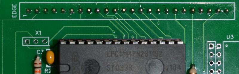
Few things have had the impact on electronics that printed circuit boards (PCBs) have had. Cheap consumer electronics would not be as cheap if someone still had to wire everything (although by now we’d be seeing wiring robots, I’m sure). Between removing the human from the wiring process and providing many excellent electrical properties (at least, on a well-designed board), it isn’t surprising that even the cheapest examples of electronics now use PCBs.
For many years, the hallmark of being a big-time electronic hacker was the ability to make your own PCBs. There have been many ways that people have tried to bring PCB manufacturing into the hacker’s garage: stick on decals, light-sensitive blank PCBs, and even using laser printer toner (that last one spurred me to write a book on PCB layout many years back). You also see a lot of people using 3D printers or CNC mills to create PCBs. Hardly a week goes by that someone doesn’t ask me how to make a PCB in a home or small business lab.
My reaction is invariably: “Why?” Back in the 1980s, I worked for a company that had PCBs made and our board house was going out of business. So we bought them. They had an array of plating machines, photoplotters, and exotic chemical handling equipment. They were 60 miles from our company, and that was handy because we’d drive over carrying giant rolls of artwork directly to the board house. The cost was high, and with modern-day regulations on dumping chemicals would probably have been higher. The price for tooling was especially high. That first board cost a lot. Even the 100th board was expensive by today’s standards.
I did a lot of boards myself in those days, especially prototype boards that were likely to have issues. But they were never the same as the commercial boards. It is hard to do two sided boards (not impossible, but hard). You don’t get plated through holes, so you have to use wires or rivets to connect the sides. You may not have thought of it, but that copper connecting both sides on a commercial PCB add a lot of strength to the PCB tracks. Just like single-sided boards are easier to delaminate than a double sided board, my homemade double sided boards had the same tendency because they were basically two singled-sided boards back-to-back. You could use some noxious chemicals to sort of plate the board, but it wasn’t as good. And I never found a reasonable way to do solder mask. Silk screen wasn’t worth the trouble, although I’ve used rub on letters and later toner transfer to get a similar effect.
The worst part about making my own boards: the drilling. Those holes really need to line up right (especially IC sockets) and if you screw it up, you get to start over at step 1. Granted, you can go surface mount, but most boards still need at least some holes (even if just for vias). The second worst part was handling all the chemicals. The clear etch wasn’t too bad, but the more readily available ferric chloride stains everything! I still have some marks on my patio concrete to prove that. I never had the gall to try some of the homebrew etches because they had nasty chemicals, too.
Things are different today. You can layout your PCB totally on the computer (or even in your browser). Click a button and you can send those files anywhere in the world. There are dozens (or maybe more) board houses that will produce your board cheaply. Many of these are in Asia, but there are affordable options everywhere now. The only thing you really need is time. You can’t have an idea in the morning and look at a prototype PCB in the afternoon. But if you are willing to wait–and the wait doesn’t have to be that long–you can get beautifully produced boards at a very low cost, even if you are making only one or two boards. You’ll get multiple layers, plated through holes, silk screen, and all the other things you expect in a professionally made board.
Yes, my CNC mill will chip away copper (and end mills) and leave me with a board with no solder mask, no silk screen, and no plated through holes. I still have my tank for heating up ferric chloride (which should have the brand name Stain-it-all). But I never do that anymore. It simply isn’t worth it. You shouldn’t either. Despite the advice in the video below, the best way to get ferric chloride stains out of things is to not use ferric chloride at all!
I’m going to stop short of recommending a particular board house so I don’t get accused of advertising for any particular one. We had a Hackerchat not long ago where several people mentioned their favorites. Ask around. Or leave your favorite (and why) in the comments.
Don’t get me wrong. No one that reads Hackaday needs to be told why someone wants to build something even though they could buy it somewhere else. I do that all the time. If your goal is to learn about PCBs or hack the PCB process, then by all means, knock yourself out. But if your goal is to prototype something and the PCB is just a means to an end, dump that ferric chloride, save the end mill, and find a board house. You’ll be glad you did.


The main reason why I think this article goes against what most hacker/maker communities stand for is the fact that it actively discourages something which is central to the core tenets of hackers and makers, namely the concept that learning and honing a new skill and/or preserving older skills is in itself worth it.
By this logic, we shouldn’t learn Morse code anymore, yet a lot of us do.
The article is aimed at an “off the shelf” mentality which you will probably not find to often around here.
OP is arguing why doing DIY if you can do it crappily. With this I agree. Point is, you don’t have to do it crappily.
He is still stuck in 1980’s with his methods. Even cheap inkjet can do really well photosensitive films, commercial proffesional chemical components are not that expensive, and whole process can be monitored and driven in much tighter limits, which gives you much more repeateble results of much higher quality.
His assertion that dual sided PCBs are some problem is telling. If you don’t have two left hands, dual sided baords are simple. Likewise with drilling. It’s not that hard to prepare things so holes can be drilled perfectly for all practical purposes.
Even soldermask is not that hard.
Don’t be in such a trouble now. Open this site directly. What you want to order on the PCB can be customized.
BTW: DIY boards have their place, even if I could find a place that would do one-off for free: I can have the board within an hour and test it immediately. This means that I don’t have to triple check everything and then worry for a month until PCBs come back.
This also means that I can skip expensive prototypes and go for bigger order confidently, since I know boards work even in the case I need proffesional boards. Often my boards are than good enough to warrant initial deployment, so I can stave board order for v2.0, if they become needed even then.
I agree with the author about three points: FeCl is crap, and so are pre-sensitized boards and hand-drilling. But making your own PCBs absolutely isn’t. And it’s not hard, either. I’ve gone from zero to double sided boards with 5/5mil features and plated through holes and vias in about 6 months. I’ve built all required tools for next to nothing, and all chemicals and other sundries I use are cheap and reasonably safe. And the price of a single board is hardly measurable.
Aside from the fun of learning the whole process, the main reason to re-start making my own PCBs was the observation that every first version of anything will have bugs. Given my low tolerance for frustration, I decided, instead of waiting another 8 weeks for another (perhaps still buggy) revision, to give home etching another try, after I swore to myself never to do it again 25 years ago. I even have access to a PCB mill, but I still chose to go down the chemical route, simply because it doesn’t constrain my designs to single sided boards with fairly coarse features. I still use the CNC for drilling, though. And I admit that without that capability my whole process would fall apart.
But I don’t regret doing it, because nothing beats the feeling when you show off a home-made board to other geeks and they all go, “Nah, dude, you just had that made w/o silkscreen to f*ck with us, that’s totally not home made!” When I first saw the cross section of a home-plated 0.3mm via in a 1.6mm board, I was literally choked up with tears of joy. I thought, that was what hacking was all about.
“Stain-it-all” Yes! Running to the Trademark field office right now. Ha.
It’s always nice how some people take a look at their own situation and then jump to the conclusion that everyone else feels like them, too. Only because YOU happen to be able to get your boards made and delivered within less than a week does not mean others are. How long it takes me if I order a custom board design? Four weeks top, but six to eight is a good estimate if I have to order from china. At least the shipping is free. Or I could order from the US or Europe, then it would be more like 2-3 weeks… plus up to $20 shipping. ARE YOU NUTS?! Home etching is alive and kicking! And if you don’t like FeCl3 stains or having to dispose off your etchant, take a look at the fully regenerative CuCl2 process!
I admit. I’m working my CNC to be able to machine accurately to cut PCBs. Because for one off prototyping, I’m cool with vacuuming up PCB dust (It’s going into a box), if/when they need more, happy to send off for dfrobot, pcway, oshparks depending on number of boards needed and time frame. get quotes off all three, and find the cheapest with the fastest turn around you need.
Your article failed to mention upcoming PCB printers. True, they don’t do the holes for you, but if you’re using SMT chips this might be the way forward: http://cartesianco.com/
Those guys are drinking some seriously expensive coffee! (“print circuits for coffee money, in coffee time”)
Adding to all the things already said: sitting in Europe (where labor is expensive (which is a good thing) and so are PCBs) why should I have someone send me something over thousands of kilometers which I can do by myself faster and cheaper? And do it again next week for the next board and again the other week? From an environmental perspective this is damn stupid. Although it’s fun to create new things especially with electronics, we should have a look on all the costs, not only financially. Shipping single PCB around the planet which could be easily made nearby is a bad idea.
I ordered some PCB from a local (Thailand) producer that can do single sides PCB or double side but NO plated holes. He is very cheap but I do not know if he can deliver oversea. He can do silkscreen but that is charged extra and is expensive. Anyway i ordered a single piece of a sigle side PCB 67×67 mm NO silkscreen NO soldermask price: 1.7 $ plus delivery expenses. He did the part in one week. His email is layercircuit@hotmail.com
“Why are You Still Making PCBs?”
I would have thought the answer was obvious – to have them made is outrageously expensive (to a large extent due to shipping costs) and involves a long lead time – what am I missing?
Interesting to read everyone’s comments on this. I work for my Dad who started an electronic manufacturing company in 1977 and he began doing what he does by making things for himself. I don’t doubt for a minute that if you want to produce a product for sale, or in large volumes, then you’re best going to the professionals, not least so that you can produce product which is ISO quality assured, but if you want to develop your interests and learn new skills then DIY is definitely the way forward.
This enabled us to accomplish the 50 µm line and space for the first time in the world as the desktop PCB prototyping machine.
http://www.mitspcb.com/edoc/fp21t_p.htm
Why am I doing PCBs at my home workshop? Because it’s fun, a lot cheaper than buying over the web and in 15 minutes I have my PCB ready in front of me. Toner > Laminator > sponge scrubbing corrosion. And I don’t have to pay shoot to nobody nor wait. And then I can have a PCB such as this in my hand quickly: http://imgur.com/dp7Us1M
I wonder what kind of mentality expects that everyone has access to a “board house”? “Boarding house” maybe “Bordello” maybe, but “board house”? you have got to be kidding.
I found another brilliant method to make pcbs at home. Do check it out as well http://www.nerdschools.com/2017/08/home-made-pcb-boards.html
I benefited a lot by the forum’s guidance re making pcbs at home. Right now I am buying ready-made PCB blanks, but I wish to make my own copperclads. I have no knowledge of what kind of adhesive bonds copper to fiberglass, phenolic sheet etc. Can someone please suggest the right kind of adhesive for the purpose
Hi, H S. When blank FR-4 PCB material is made, it’s made from laminations of fiberglass cloth and epoxy, and it’s this epoxy that also adheres the copper. For phenolic PCBs, the laminations are paper or canvas, with phenolic resin, and again, the phenolic resin is what adheres the copper to the board.
I Thank you very much for your kind response, BrightBlueJim.
I am aware of only Araldite brand which as you know well, is epoxy and hardener supplied in two different tubes which mixture I have used successfully to bind a wide variety of other materials.
The huge problem with Araldite in my experience is that Araldite bonds everything except copper foil which fact has been a great disappointment for me. I tried this several years ago and quite recently too. Before bonding, I do clean the copper foil using household detergents (such as everyday utensil cleaning powder and cloth washing detergent), using Scotchbrite and drying the foil well; but still I cannot understand why copper refuses to bond with phenolic board with Araldite. On bonding to copper and waiting for 24 hrs, the copper foil comes off the base easier than orange peel.
May be I am not using the right technique. If Araldite does not work, please could you direct me to any brand name of phenolic resin. An ordinary trader in India may not understand what is a phenolic resin unless an accurate brand name is mentioned.
I have come across a product called Fevicol Heatex. Is this adhesive worth trying ?
Looking forward to receiving your further guidelines.
Kind regards
hsdhar6@hotmail.com
29/12/2017 8:45am
I don’t know whether the problem you’re having with epoxy is with the copper or the phenolic, but I suspect the latter. I don’t have any experience with phenolic resin, so I can’t advise you on that. HeatX is a synthetic rubber contact cement, which SHOULD adhere to both, but my concern is whether it could handle soldering temperatures. It’s advertised as good to 170 degrees C, but that’s below the melting temperature for lead-free solder (183degC). Which might still work, but it’s something you’d want to test before committing to a full circuit board.
Part of the fun is figuring out all the different ways to do home made PCBs – appreciate
human ingenuity – it’s kinda the best of times, the worst of times – some things have become
awesome for DIY (3D printers, the information on the Internet, cheap parts from China), but
the disappearance of local shops , diy friendly components etc is kinda bad.
On the topic – Incredibly , folks have discovered using Mosquito Repellant for Cold toner transfers – worth a dekko –
[youtube=https://www.youtube.com/watch?v=ICN15_0Mb_U&w=470&h=295]
[youtube=https://www.youtube.com/watch?v=1oRYKKIqBOE&w=470&h=295]
Thank you BrightBlueJim
Copper foil not sticking to phenolic board – still an years-old mystery to me.
Readymade copperclads are getting expensive by the day. Just last week when I enquired around, a 7×6 inch blank is priced in the retail at twice the total cost of the components that I propose to mount on it, hence my hue and cry about coming up with a home-brewed laminate.
Good old FeCl3 + nail polish masking + nail polish remover is still working great for my DYI purposes.
Tomorrow, just with a view to gaining some addl experience (and being DYI-oriented), I am going to try the flg:
Experiment #1:
A thin asbestos sheet as a rigid substrate + Araldite adhesive + copper foil + the usual etching technique as above. This should work to my satisfaction – hope you will not laugh at my off-beat approach towards this experimental combo; but it sounds better than spending a fortune on the readymade copperclads.
Asbestos being a health hazard, I am going to paint up the finished board with a heavy layer of heat resistant, lead-free paint.
Experiment #2:
A thin glass sheet + canvas sheet in between the copper foil and the glass sheet (soldering heat shield) + Araldite + the usual etching work with FeCl3; no attempts at boring holes on the substrate – (being glass), soldering the components directly on to the copper tracks on the drawing side (surface mounting – sort of !?). This DIY approach is just for observation and of course preserving the assembled board to posterity!
Here is what I will do next:
I have salvaged some PCBs from a good old television set, and hopefully after etching away the existing copper tracks on them, I will try pasting up an entirely new copper foil on to the bare phenolic base sheet, and then shall proceed with the usual etching work for a new circuit.
As you have kindly indicated, it might be worth trying Fevicol Heatex. I shall try that in the days to come. I am quite eager to share my observations with you.
My thanks also to the other forum members for their valuable inputs and for sharing their personal observations.
Mosquito repellants, cold toners? Unfortunately, my browser could not open the page posted by QuadTech. Hoping to view the contents some other time.
With kind regards
H S Shridhar
Bangalore, India,
30-12-2017 08:50am local time
hsdhar6@hotmail.com
I found a bit of double-sided 3M adhesive in my junk box.
I stuck one side of the tape to a thrown-away plastic lunch box and on the top of the stick tap, I affixed copper foil strips as per the circuit requirement, and soldered on the component leads with a 35W soldering iron. The soldering happened perfectly well with the copper did not lift up from the base, in other words the tape’s heat tolerance was quite good.
The monkey grip of the 3M on the plastic base should be felt to be believed – such a strong bond, indeed, but it is a question of time – how long the 3M tape will remain stuck to the plastic base.
But I did not at all like the squishy, spongy feeling of the tape underneath as I went on soldering the joints, but the compromise was worth the outcome.
I also wanted to test the tape’s limits by jabbing my 65W chassis basher to try and de-solder as a trial, but I did not have a heart to do so at least for the time being; I will try this some other time, in case I need to proceed with de-soldering.
I am just trying to save money by avoiding the ready-made copper clads.
I do not know how to thank Hackaday and the forum members for their invaluable inputs.
HSS
Bangalore, India, 02-01-2018 9:45am local time
hsdhar6@hotmail.com
PCBINDEX was founded in 2006,Headquartered in Shenzhen, China. With over ten years of experience in PCB(including PCB prototype) field, we are committed to meeting the demands of customers from different industries in terms of quality, delivery, cost efficiency, ect.. As one of the most experienced PCB manufactures in China, we take pride in serving as your business partner who can supply the PCB products which are exactly what you need. http://www.pcbindex.com
Sometimes there is a need for simple pcb’s, fortunatly there is another method: https://www.instructables.com/id/Making-A-Customized-Circuit-Board-Made-Easy/.
As far as the FeCl3, there are other oxidizers available. Such as peroxide with hydrochloride acid as activator. When the solotion is no longer active the copper in solution can be removed by adding NaOH and the filtrated out. Or it can be removed by electrolosis.
if the solution is copper chloride I would think that a more active metal would work no matter what, so going straight to sodium in the sodium hydroxide seems extreme, I have made zinc sulfate and copper oxide from brass, just by tossing the whole mess into sulfuric acid, because the zinc is more reactive and so all the sulfur is attached to the zinc until the zinc is completely used up, even if the copper is attacked first, as it just swapped places with the zinc once it was in contact with it, just don’t use turned shavings off a lathe if you used an oil coolant, then leave it sitting on a shelf thinking it will be fine, because it is only half full of liquid, as I did.
You will come back a couple months later and find a ton of zinc sulfate stuck to things, and the jar will be filled to the brim with some running down the edge due to the high hygroscopic nature of the zinc sulfate, and the oils ability to retain that water so it does not easily evaporate back off during dryer moments it seems, lol.
PCBs applied in vehicles are the fastest growing sub-industry
Auto electronics are developing into the following six directions: mobile communication, multi-media entertainment, safe driving aids(including automatic driving), riding comfort and convenience, energy saving and power saving(electric cars), which all poses many challenges to the PCB industry as well as providing good development opportunities. For example, automatic driving will bring about the large-scale applications of millimeter-wave radar, therefore, the demand for high-frequency PCB circuit plates which are suitable for radar will increase significantly as its value are apparently higher than that of the traditional PCB plate. BMS is one of the core parts of the electric cars, while the PCB plate is one of the basic parts of BMS, which may also benefit a lot from the development of electric cars. Currently, vehicle-used PCB account for around 2% in the entire car electronics as well as around 10% of the total PCB industry, whch is not the highest but is the fastest increase rates. According to predict from Prismark, the compound growth rate of vehicle-used PCB is high as 5%, which is higher than that of the overall PCB industry.
Automotive electronics’ demand for PCB is diversified: a co-existence of demands for products with the lowest price and the most reliable/security degree. Hard plates are widely applied in applications, such as, instrument plate, vehcle-used sound system, car-used comuters, which makes the four-layer plates account for the largest part with a proportion of 38%, two-layer ones and six-layer ones account for 16% just secondary to it and 5-layer plate accouting for 5% next to that of the two-layer and six-layer ones. In terms of applications in engine room, PCBs applied in Radiating ceramic substrate accounts for 3% due to the cooling requirements from the hot temreture environment and LED lighting source. In terms of high-frequency transmission and wireless radar detection, Low Temperature Co-Fired Ceramic( LTCC) accounts for 5%. The products which are particularly developed to meet the demands of cars(such as IC support plate , soft plate, penetrating holes with elargol, etc.. ) account for 17% of the PCB application. On average, one square meter of PCB plate is used in every car, with a value of around USD$ 60.
Driven by the electronization of cars at large, vehicle-used PCBs will also increase. Vehicle-used PCBs are characterized by having steady order and high gross profit rates, which have drawn great attention from many PCB insiders to this new blue ocean. Vehicle-used PCB are mainly oepratd in a high-speed context, which made the requirements for this kind of PCB higher than that of ordinary ICT products specifications in terms of temperature resistance, electromagnetic waves proof, earthquake proof and corrosion resistance. As a result, to guarantee the quality of car parts and ensure the life safety of driving and passengers is an important issue faces by all the car manufacturers; whether car parts vendors can provide a long-term and stable quality is far more important than that of the low-price ones. Besides, the car manufacturers’ inspection for products tends to last as long as three years. Therefore, PCB manufacturers who would like to march into the car electronic syply chain usually need more patience and strength. http://www.pcbindex.com
Where is possible to request naked PCBs in single and double face, in Europe?
Eurocircuits extinguished the service (they claimed the low demand, but if there was little demand it is because the orders were tabulated and could not be in more than 5 units and because they did not allow to make a panel with different types of layouts / PCBs and was not available for simple face pcbs. With these limitations it is natural that the demand for this service was few and often simulated with the proto pcbs, and naked pcbs come out almost more expensive than a proto pcb with all the extras, very strange! I did not ask for more, because of these limitations and the little discrepancy in prices against the complete PCBs.)
>WHY ARE YOU STILL MAKING PCBS
Because they are too expensive to order, obviously.