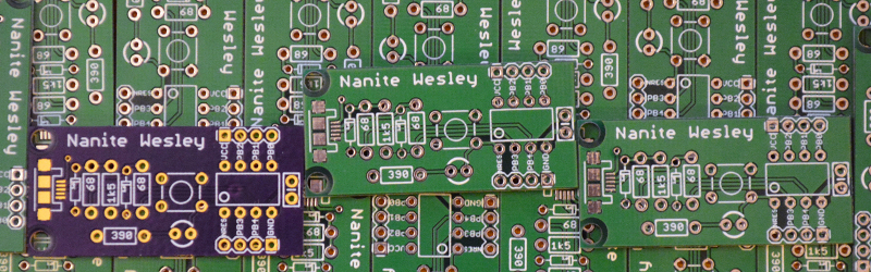
This is the continuation of a series where I create a PCB in every software suite imaginable. Last week, I took a look at KiCad, made the schematic representation for a component, and made a schematic for the standard reference PCB I’ve been using for these tutorials. Now it’s time to take that schematic, assign footprints to parts, and design a circuit board.
All PCB design tools have different methods of associating the schematic view of a component with how it will be represented on the finished board. Eagle uses libraries that contain both a schematic view and PCB view of a component. In the prehistory of PCB design software, Autotrax simply ignored the schematic view.
KiCad has a clear separation between a symbol (the schematic view) and a footprint (the PCB view). If we were to take our schematic and create a new PCB by running PCBnew, nothing would happen – our symbols aren’t associated with any footprints.
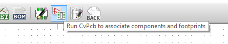
To associate symbols with footprints, we need to run CvPCB. This sub-program tucked inside KiCad gives us the ability to associate footprints with our schematic symbols.
It’s like the cloud, only not completely worthless
CvPCB is a new feature for KiCad 4.0. Instead of every other PCB design tool we’ve taken a look at so far, KiCad effectively stores all of the footprints in Github. In the Github repo for KiCad, you’ll find a bunch of files with a .pretty file name. These are the footprints for nearly every component you can imagine. If you’re running a fresh install of KiCad, everything shows up in CvPCB automagically – there’s nothing you need to worry about, and footprints just happen.
There’s a subtle brilliance about this implementation. It’s like the cloud, only it’s completely verifiable, and if a part doesn’t work, you can fix it and submit a pull request. Already, this is phenomenally better than the Eagle paradigm, where millions of footprints are available in thousands of different libraries scattered around the Internet. If you’re reading through this series in order, take note: this ‘Github as the cloud’ will be a major point of comparison when we get to other cloud-based PCB design tools.
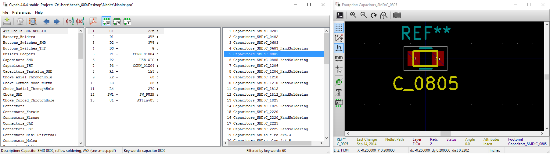
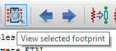 With that said, we need to associate footprints with the symbols on our schematic. To do that, go down the list in the center of the CvPCB window that contains a list of all the components in our schematic and associate a footprint with each part. Footprints are on the right, libraries (or categories) are on the left. To view the selected footprint in a new window, click the ‘view selected footprint’ button.
Getting Libraries In Order
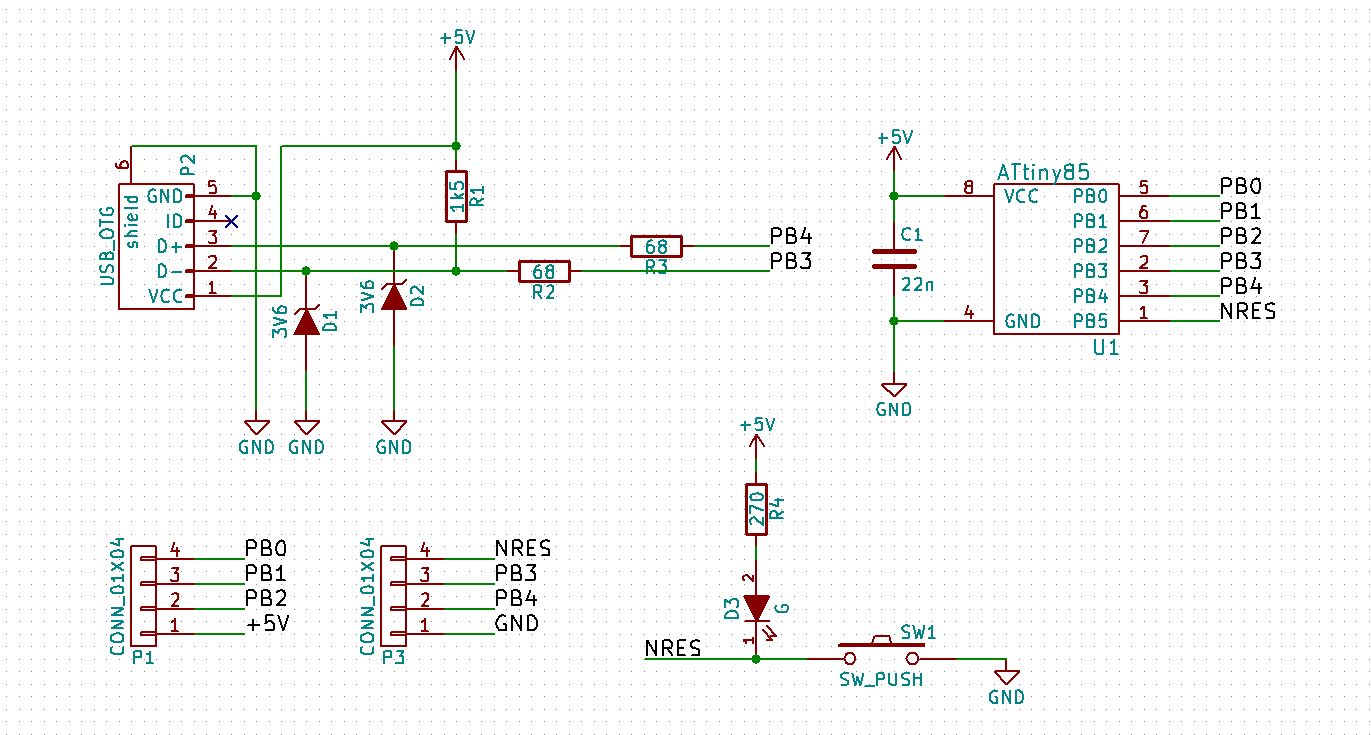
This project is using (mostly) all through-hole parts, and as such, I could easily select a DIP8 footprint for the ATtiny85 and be done with the whole thing. This is a tutorial, though, and I need to demonstrate how to make a part – schematic and PCB view – from scratch.
To make a footprint, KiCad offers a Footprint Editor. This can be accessed from either PCBnew or the launcher. Click on that, select File -> New Footprint, enter a name for this footprint (‘ATtiny85’ will do), the name of the footprint and a reference designator is placed onto the footprint editing window.
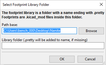 Libraries are important, and since KiCad is now running on ‘not-worthless cloud technology’, we have to create a library for this project that won’t be saved along with our copies of the standard Github libraries. Select File -> Save Footprint In New Library, save this library wherever the rest of the files are for this project, and give the library a name.
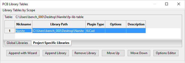
We have just created a new library, but that doesn’t mean KiCad knows what library we’re working with. In the Footprint Editor, select Preferences -> Footprint Libraries Manager, and click on the ‘Project Specific Libraries’ tab. Hit the ‘Append Library’ button, and drop the path to the library we just created in the ‘Library Path’ field. That’s more KiCad weirdness, but once we’re done we can finally create a footprint.
Making The Footprint
Now that we have the Footprint Editor open, a part name and a reference for the footprint, and the library all set up, it’s time to actually put some pads down. There are a few relevant buttons on the screen:


The most important, obviously, is the ‘Add a pad’ button. Click that and drop some pads down where they should be. This is a standard DIP8, or two rows of four pins 0.3″ apart. The default grid, as you may have noticed, is 50mils.
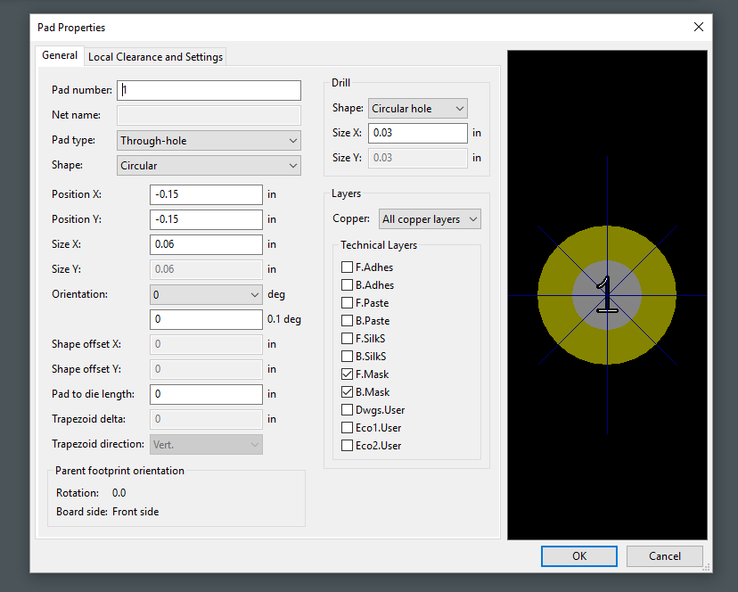

After placing the pads, use the hotkey ‘E’ to edit the properties of each pad. Here, you can change a through-hole part to an SMD, change the dimensions of the pad, hole, and shape of everything. Importantly, the Pad Properties window allows you to change the number of the pad. The number of the pad is how KiCad connects the schematic representation of a part with the footprint. Get this right, or else nothing will work.
Add a few lines to the footprint, save your work in the project library, and go back to the schematic. You’re done. That’s how you make a footprint.
From Schematic To Board
Now that the schematic has footprints associated to everything, it’s time to open up PCBnew, move parts around, and put some traces between parts. Do that. Oh, nothing shows up. Why is that? You need to generate a netlist in the schematic view, and import it in PCBnew. There’s a button with ‘NET’ written on it in both programs. Click those. Now, what do we get when the netlist is successfully imported into PCBnew? The worst mess you’ve ever seen in any sort of design program:
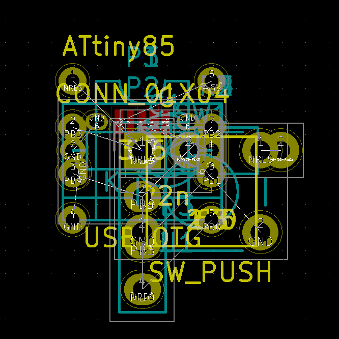
 We end up with a gigantic mess on our hands. No worries, ‘M’ is the hotkey to move the parts around. You can also use the ‘Move Footprint’ mode to automagically place these parts. Reference the PCB we designed for the introduction to this series and move some parts around until we get something resembling the board below. The relevant hokeys are ‘M’ for move and ‘R’ for rotate. As always, there’s the ‘?’ hotkey that tells you everything you need to know.
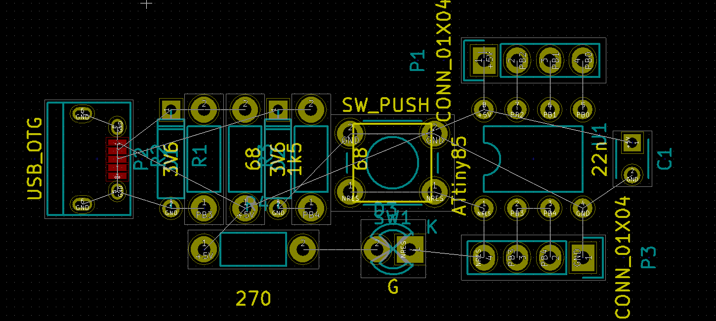
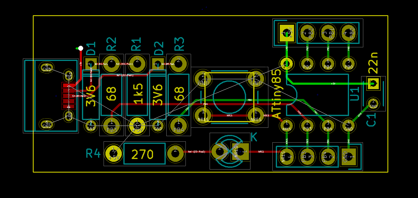
That’s close, but it looks horrible. Deselect Footprint mode, use your cursor, and move all those labels and references around. We don’t need “CONN-01×04” on the board, and it’s really helpful to have the values of resistors inside their own footprint. With a little bit of work and deleting those labels, you’ll have something that looks like this:

Holy crap, that actually looks like something. All the resistors and diodes are labeled with their value, all the superfluous references are gone, and this actually looks good. You can’t do this in Eagle easily.
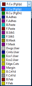 With the layout pretty much figured out, it’s time to finally draw some traces. This requires a description of the layers.
- F.Cu and B.Cu are the top and bottom copper layers. The hotkeys for these layers are PgUp and PgDn
- Edge.Cuts is the equivalent of the ‘Milling’ layer in Eagle. This is the outline of your board.
- F.SilkS and B.SilkS is the silkscreen – the text and outlines of your components.
- F.Mask and B.Mask is the soldermask. It’s usually green, or purple from OSHPark.
- F.Adhes and B.Adhes is glue applied to SMD components.
- F.Paste and B.Paste is where solder paste will be applied.
For a simple board that won’t be sent off to an assembly house, the only layers you need to worry about are the copper layers, the Edge.Cuts, and the silkscreen.
The first thing to do to complete the board is to draw the ‘edge’ or milling layer. Select the ‘Add a graphic line’ button on the right hand toolbar, and draw a rectangle around all our parts. That’s simple enough.
Now it’s time to actually put some traces down. You can select which copper layer to use in the top toolbar, and the relevant hotkey is ‘X’. Hit ‘X’, click on a few airwires, and route them just like the reference PCB. Don’t worry about power or ground traces – we’re going to do those with copper fills. When you’re done, you should have something like this:
 That’s pretty much all there is to it, save for the copper fills. To do that, we need to add a ‘filled zone’ or ‘copper pour’ or a ‘polygon’. By any other name, it’s just a big area of copper that is connected to a single net in the schematic.
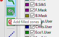
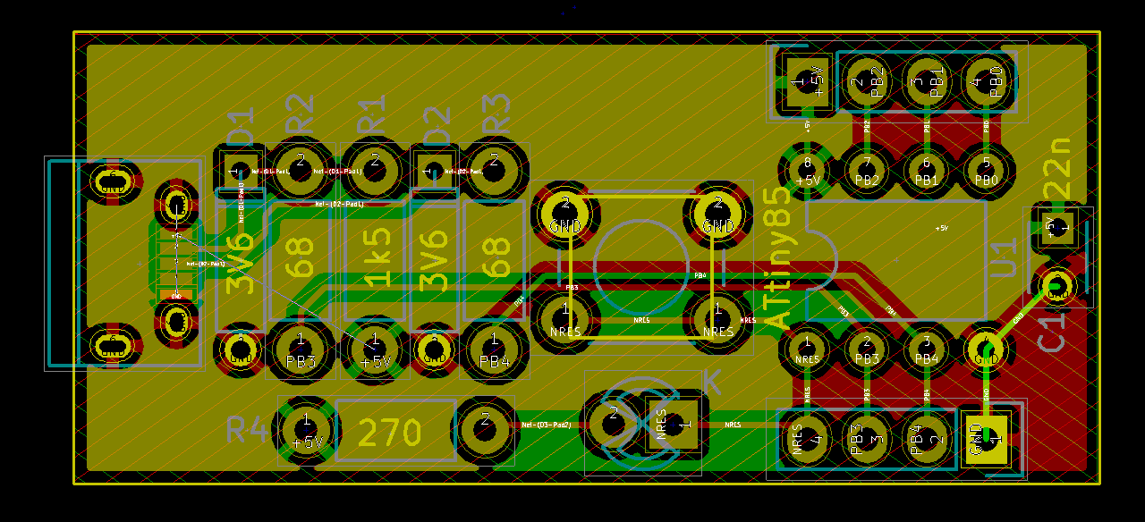
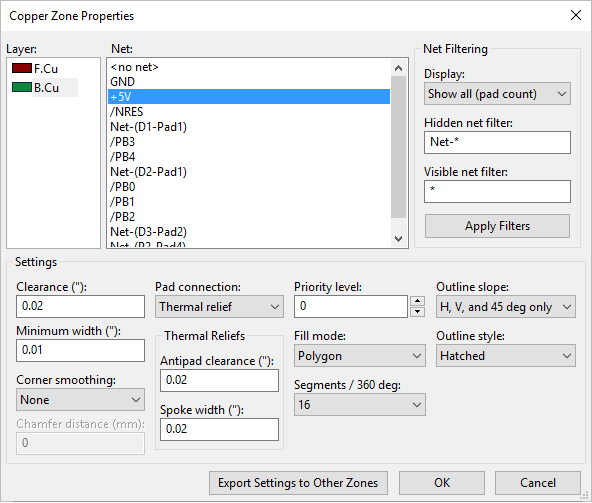
Click on the ‘Add filled zones’ button, and a ‘Copper Zone Properties’ window will show up. Here, you can assign a layer of copper to a specific signal. Our board puts +5V on the back copper, and GND on the front copper. In the Copper Zone Properties, select the B.Cu layer, the +5V net, hit Ok, and trace around the edge of the board. Do the same with the F.Cu layer and the GND net. When those fills become hatches around the edges of the board, hit the ‘B’ hotkey to render the copper fills.
That’s it. We are technically done. If you save and drag the .kicad_pcb file onto the OSHPark web page you’ll get a pretty purple PCB in a week or two. That’s not to say this PCB actually works – I screwed up the USB signals in the schematic, and that propagated over to the PCB. No matter, because no one is actually going to build one of these boards.
This just about concludes the ‘Creating A PCB in Everything’ tutorial for KiCad. If you’ve been reading along for the last five thousand words, you have an excellent introduction to KiCad, and should at least be able to build a breakout board. This doesn’t mean I’m done with KiCad quite yet – there are a few more tricks to go over including DRC and ERC, a demo of how freakin’ awesome the routing in KiCad is, and I need to put a keepout on the decoupling cap in on the board, anyway. Creating a PCB in Everything: KiCad Part 3 (the optional part) will be out sometime next week.
Thoughts on KiCad
This series of posts serves two purposes. First, it is a quick tutorial for various PCB design tools. After reading these posts, you should be able to guess your way through a PCB design tool and build a simple PCB. Second, each of these tutorials serves as a pseudo-review of each PCB design tool. Each of these posts serves to illuminate the quirks of a PCB design tool, and serves as a notice that I still have an unclaimed bounty for the first person to create a part for an ATtiny85 from scratch in Fritzing. Don’t use Fritzing, it sucks.
Coming from Eagle, KiCad is downright weird. That’s not to say it’s difficult, though – it’s generally the same as any other PCB design tool. The interface, like nearly every Open Source project, is obtuse, and there are five non-obvious ways to complete any task. There is zero reason why parts imported from a netlist into a board are squished together. Custom libraries can and should be automatically imported. The KiCad community especially rancorous. The UI suffers from an intangible wrongness about it, although that seems to lessen after working with it for a few hours. In a sense, KiCad is exactly what you would expect from an Open Source project that is decades old, very mature, and has features packed to the gills: it’s very powerful, but not friendly to the beginner.
Although the KiCad beginner will struggle to wrap their heads around the interface, it will be one of the most powerful PCB design tools I’ll use in this series of posts. No other free (beer) program will give you 32 copper layers and unlimited routing space. Nothing else uses the cloud/GitHub like KiCad. It’s brilliant.
A few months ago, if someone asked me to suggest a PCB design tool, I’d give Eagle or KiCad as suggestions. Eagle is easy enough to learn, and will be getting better since the Autodesk acquisition. KiCad is robust, and even in the best case of Eagle development, Autodesk may only ever reach parity with what KiCad can do.
Now, KiCad is growing on me. I have a secret project where I need to build and manufacture a thousand relatively complex boards. My previous go-to was Eagle, but I think I’m going to do this board in KiCad.


Nice although I see the “cloud” doing for PCB design what Google’s “warehouse” did for Google Earth. Leveraging all that talent out there.
I think Brian’s view on the quality of the prefab Kicad parts is a little overstated… I think the /real/ benefit is you can make all the footprints you need in KiCad crazy fast, so it doesn’t matter if the specific part you need has a footprint or not.
That’s true… I’ve done about 5 commercial boards in KiCad from low complexity to about as complex as you would want to do on a 2 layer board. And I tend to either make my own parts or import them into a local library so they don’t get screwed up over time as they get updated (once I have something that I know works why would I want to change that).
Making my own parts bit me once more than I would have liked or expected an FA-238 cyrstal needed a bit more separation between the pads + less removal of the solder mask around the pads as what occured is that there was such a small gap that about 1-2 out of 10 boards the crystal would short itself out and kill the board.
So, scratch the traces and add epoxy? Or was it a destructive event?
The biggest benefit I see to KiCAD (that I don’t see mentioned often) is the files are plain text and the formats are very simple. This means one can easily create programs (say a Python script) to create and modify these design files without opening KiCAD. Example automate the creation of multiple footprints given an user defined algorithm.
More examples:
http://www.xess.com/blog/giving-back-to-the-community/
https://xesscorp.github.io/KiCost/docs/_build/singlehtml/index.html
https://xesscorp.github.io/KiPart/docs/_build/singlehtml/index.html
https://github.com/pointhi/kicad-footprint-generator
http://kicad.rohrbacher.net/quicklib.php
http://kicad.rohrbacher.net/quickmod.php
Here’s an example of another project at that generates KiCAD schematics from Python
“SKiDL is a module that allows you to compactly describe the interconnection of electronic circuits and components using Python. The resulting Python program performs electrical rules checking for common mistakes and outputs a netlist that serves as input to a PCB layout tool.”
https://xesscorp.github.io/skidl/docs/_build/singlehtml/index.html
To take care of “The worst mess you’ve ever seen in any sort of design program:” ,
Select Footprint Mode
Context click over any one Footprint
Select Global Spread and Place > Spread out all footprints
This makes it easier to select and move footprints.
I also learned it sorts based on annotations so everything with a 1XX, 2XX, 3XX etc clumps together. This makes it easy to separate circuit block for routing them one by one
The unstable version spreads the components out automatically, so it’s not going to be a problem all that much longer anyway.
I only use the ustable version, stable still needs to get STEP support and rounded corner pad support, those are essential for design for manufacture.
This is automatically done on netlist import. It is so much better, but has been stuck in the dev version for the last year. Hopefully KiCad 5 comes out in the next few months. Quite a handful of small workflow issues like this have been improved.
It is important to mention that while the *official* footprint/symbol repositories are in Github, nothing forces you to use them online, unlike some other tools which are “cloud or bust” system (i.e. cannot be used without internet access).
In fact, it is much faster to simply download them locally and point Kicad to the copy instead. That has also the advantage that the footprint won’t change behind your back because someone has updated it online.
I made a repository of all the footprints I know of for just that purpose: https://github.com/monostable/kicad_footprints#kicad-footprint-collection
There is that wonderful “Save a local copy to:” checkbox in the footprints wizard.
and “archive footprints to project library”
” That has also the advantage that the footprint won’t change behind your back because someone has updated it online.”
Isn’t that why you create a local library and copy the footprint into it?
“Last week, I took a look at KiCad”
*Three weeks ago
sockwatcher…
“You can’t do this in Eagle easily.”
Actually you can. Any component on the board view can be “smashed”, which separates the component name and value from the part, and those can be moved, resized or deleted individually.
I am always using the smash command, especially because all of my layouts are SMT and I don’t want the silkscreen ref des underneath the part footprint. I wish there was a way to unsmash the part so it could regroup all the ref des with the part again when I move it. I don’t think there is though?
There is a way to unsmash. See help SMASH, if memory serves it’s a shift+left click with the smash command active. You can also go into the Properties dialog and uncheck the smash check box.
Best Regards,
Jorge Garcia
Autodesk Support
If you right click on the component “cross hair” used to move the component around, you can select “unSmash” and it will pull all its labels back to the default locations.
You can also do this to the entire design (or a portion of it) by selecting “Smash”‘, then “Group” drag to select the group then right click on a selected item and choose “Group: Smash”
(that same thing you use to move groups of parts can be used to delete them, copy them etc)
His weeks are not like our weeks…
Is this like the difference between “schedule weeks” and “delivery weeks?”
November 17 sure does feel like “last week” :)
Good contribution to the comments section! I’m always impressed by the great community we have here!
So, with that out of the way, I *wrote* this a while ago. It’s been sitting in pending for a while. The reason for that is because the first KiCad post didn’t do so well in terms of views and clicks.
This surprised me, because for all of these ‘Creating a PCB’ posts, the one constant was a request for a KiCad tutorial. For every single post in this series, people have been requesting a KiCad tutorial. Strangely, the post on Autotrax – a tool no one should use in $CURRENT_YEAR – did significantly better than the first KiCad post. Weird, right? Why on Earth would people say they want to see a KiCad post, but not follow through with reading it? Bizarre.
It’s almost like when people say they don’t want to read clickbait headlines, but those headlines always bubble up to the top of your favorite news aggregator. It’s almost like people saying the Discovery Channel has gone downhill because it’s all Ice Pawn Crab Truckers, but that’s actually the most profitable thing for the Discovery Channel to air. Weird, right? People say they would like to consume a specific piece of content, but then they don’t follow through. Strange. Inexplicable. I can’t wrap my head around it.
You want a reason why this post has been kicking around in the pending folder for a few weeks? It’s you.
Geez, calm down, man. You’re always so hostile like this, it almost seems like you’re trying to drive people off.
Well I feel honored and special, despite the (probable) sarcasm and verbose response. Incidentally, I have been meaning to complete a board in KiCad after Drew Fustini of OSHPark encouraged me to do so and I had your November article bookmarked since it came out. In fact I read through it last night to get started, wondering where part 2 was. Well, here it is and thanks! I am still not confident that my design will be easy to complete, but the crash-course has been helpful to understand the gist of it.
As an avid HaD reader I must “Thank You” for your work on these two posts on KiCad and I’m waiting for the next one. I never asked for a KiCad tutorial since I have been using it for a few years now but still enjoyed reading every single word and some helpful comments from some users. Will certainly forward it to some friends. Why didn’t it get more views? Maybe the usual TLDR? I guess most people just prefer to watch what others do than to learn so that they can do cool stuff as well. Congratulations for your work and I hope the low number of views don’t stop you from writing this kind of posts in the future.
People that have not used KiCad before or are sitting on the fence before choosing a new program will click immediately. People already familiar with KiCad will think “cool, I’ll read that one later.” If it is something I’ve never seen before I’ll look at it now. Paying per clicks is not fair to the HAD writers.
It would be nice to be able to up vote posts to a reference or tutorial category or heading and pay more for those write ups that took extra time and thought.
> Paying per clicks is not fair to the HAD writers.
What the hell are you on about?
Take two hypothetical “writers” (to use the term loosely).
One writer spends a week working on a post for a tool that contains good information, knowledge and is useful to the community. Another writes a click bait article in two hours talking about how the whole premise of Linux is a trap designed to frustrate the open source community and force everyone back to using Windows and MacOSX.
Which “writer” will get more clicks? Which will make more per hour?
People don’t know what they actually want. If you ask what people want they will describe what they already know but why would they read about that?!?
Good article, thanks for your work. By the way my google app suggested your article.
Lol, just wanted to say that I would watch “Ice Pawn Crab Truckers”, that sounds awesome.
EDA tool tutorial is not the kind of article you want hundreds of comments about, at least not instantly. People need a lot of time to process this kind of material. If someone was waiting for your tutorial, they are now waiting to have free time and inspiration to follow it. In its due time it will come in handy to many people.
man, Brian doesn’t take any shit. I like it.
he’s going to make the comments great again!
On having to export and then import a netlist, there is an easier way. On the schematic, instead of clicking the toolbar button to merely open Pcbnew, open the Tools menu and use “Update PCB from Schematics” (or alternatively, just press F8).
This lovely feature is only in the dev branch of KiCad currently.
Oh. I’ve never used anything other than the dev branch, because when I first started I had to choose between that or something quite old… Never had an issue with it though.
As a regular Kicad user, I cannot stress enough the point of staying away from the github versions. you don’t want your design changed because someone on the internet thinks it is a good idea to change cathode on a diode from pin1 to pin2 or v.v. That happened a while ago and will happen again as long as people are pushed to use the cloud repros by default and no clear workflow exists to only use your own parts based on the cloud version or drawn yourself.
I am still unable to get that crucial problem with the workflow across to the developers. this is especially problematic with EEschema as it automagically updates symbols in your schematic every time you open kicad.
NEVER USE THE REPROS DIRECTLY, COPY TO LOCAL LIBS ONLY.
it would be a shame to get disappointed as a new user for these easy to mess up problems.
Changes in the Repos would only affect your board if you “reload” footprints in PCBnew. It won’t touch the footprints unless you do that, and it caches the old version as well.
You probably should revision control your PCB files as well to be sure if you have old working versions of boards if you plan to redesign without checking footprints. Most are very stable things that no one would ever touch like 0402, or LQFP 64 or SOT.
As you may have noticed , i was talking about EEschema. If parts suddenly dont toch wires or pin numbers change during your designing process, you will find out during dcr that some errors dont show up. Revision control on boards is not solving this, but revision control on symbols and parts is maybe a saver, but not the solution.
Basically i hate it when things change without me doing the changing.
+1
Brian – thanks for posting all of the articles in this series. It’s great getting your commentary on the “new user” experience. Just wanted to add a few things that I’ve come across as a newish KiCad user (so apologies in advance if I’ve missed something).
KiCad’s Gerber/NC Drill output has really improved since the last time I touched KiCad (3.x?). Fills are output as irregular polygons by default (good!), as opposed to the “scan line” method used by other packages.
Things like mask clearances really work best using global settings – putting these in at the footprint really seems to be an invitation for creating output errors. OTOH, when you stick with global settings, It Just Works very well.
The ability to create XSLT plugins for BOM output is terrific. And while learning KiCad, I expected that I’d see the same for pick and place output :( Which brings me to…
.POS files. Horrible. .POS files are aptly named – there’s no CSV option for some reason (it’s just a de facto industry standard) – and it just seems to be an area that’s begging for improvement. Hoping that the plugin thing is extended.
Lastly – sure would be nice if a lot of settings could be saved in a config file that could be easily distributed. Something that exists for other packages, hope to see something like that in KiCad soon.
Anyways, outside of those issues, and some of the weirdness mentioned in the article, we’re really loving KiCad here. We’ve been seeing some months where we get more KiCad output than anything else, not surprising after having used it.
More and more PCB manufacturers are allowing custom shaped boards (e.g. Dirty PCB). Could you do a comparison of this functionality please?
It’s actually really trivial – just draw whatever outline you want on the Edge.Cuts layer. It doesn’t have to be a simple rectangle.
You need to use the push and shove router by switching to OpenGL rendering mode. It is the *best* part of the 4.0+ versions of KiCAD. You can use either push and shove for walk around mode.
– Never trust any “I got it off the Internet” library without careful testing and verification.
– Design your own parts footprints for the parts you want to use.
– Double check that the footprints match the parts you’ve specified.
– Verify that you can purchase the parts that you’ve designed the footprints for.
– Verify that the footprint can be manufactured / soldered well, for that given component, after PCB fabrication.
– Once you’ve got a production-proven footprint for a given component, you can re-use that component with confidence next time.
This is important, regardless of whether you like Kicad, Eagle, Altium, or whatever.
Clearly it’s harder to stuff up when you have very standardised footprints that are always essentially identical (like an 0603 resistor for example) but more important when you get to things like inductors, connectors, and weird ICs where the particular device has a bit of a unique package or footprint and there are different styles.
> There’s a subtle brilliance about this implementation. It’s like the cloud, only it’s completely verifiable, and if a part doesn’t work, you can fix it and submit a pull request. Already, this is phenomenally better than the Eagle paradigm, where millions of footprints are available in thousands of different libraries scattered around the Internet. If you’re reading through this series in order, take note: this ‘Github as the cloud’ will be a major point of comparison when we get to other cloud-based PCB design tools.
Fritzing does exactly the same thing, what a shame it didn’t get a proper review.
Fritzing is like using a sledge hammer to make jewelry; It works, but there are proper tools that make the job easier. While Fritzing can do board layouts, the real beauty in the tool is it’s simplified schematic view (or better put, its pictograph view, because lets face it, for any engineer out there, Fritzing isn’t a schematic capture tool). As such, if the footprints are or are not on a ‘cloud’ service like GitHub is irrelevant. The tool fails as a good solution to board layout long before it even reaches the point where the ‘could’ matters.
And yet there’s this:
> I still have an unclaimed bounty for the first person to create a part for an ATtiny85 from scratch in Fritzing. Don’t use Fritzing, it sucks.
Just because you didn’t like Brian’s assessment doesn’t mean it’s invalid.
Fritzing got a proper review.
Here’s the review structure for this series of posts: Take a standard schematic and board file. Re-create those in a tool, and also create a part from scratch. The Fritzing FAQ says you cannot create parts from scratch. Right off the bat, it is impossible to do what I need to do in Fritzing.
Right, so after the KiCad posts, I’m going to do the ‘how to create a part in Fritzing’ tutorial. I will shit on Fritzing throughout the entire tutorial.
You have my support!
+1
Yes! Instead of arguing which EDA tool is the best, let’s all us elite haxorz team against Fritzing. Unify the shitstorm!
I recently went to a Kicad tutorial at my local hacker space with hopes of moving to this EDA platform. As a long time Eagle user I’ll admit that I have a bias towards it. With that said I was excited that this would be the opportunity to open my horizons to this software that so many rage about.
We started with the schematic creation. That went really well. It was easy to pickup and generally made sense. I could see myself using this! The only thing that bothered me was when moving a component the wire connections didn’t move with it. I thought what was kind of odd.
With a schematic with two dozen components or so under my belt I assumed that clicking the Pcbnew button would drop me into a board view and we could start routing! Nope, I was totally wrong. There’s a whole step that still needs to be done that involves associating footprints with each component. Seriously? Why isn’t this done when you pick your components in the schematic?
Okay, finally time to click the Pcbnew button and get routing! Wait, wait it stacks the components all on top of each other? Dafuk? “So as you can see, the components are all on top of each other, you need to select them all and spread them…..” Said our instructor. Nope, I was done. This was the proverbial straw that broke the camels back. I’ll stick to Eagle thank you very much.
KiCAD is awesome piece of software. You have to find a problem between your LCD and chair… :)
I made a lot of PCB in Eagle and realy love that switch to some new SW, where I can make all much more faster with shortcuts. Eagle is quite obsolete EDA SW. No one using it at our univesity anymore.
I’m sure it is a great piece of software. So is linux but I still use windows because it just works. Kicad just isn’t for me. I’m glad you like it.
about the footprint association: thats really handy imho. you can design the schematic before thinking about the physical chip size, and if it turns out, you can’t get the form factor you initially wanted, its easy to swap out!
your instructor was wrong on the stacked components: there is a button to spread them out for you, and it is the default option when importing in opengl mode iirc.
I understand how handy it is to be able to select footprints. In Eagle I just right click in either the schematic or board, select Package and choose from the list and it updates both the schematic and board.
Yes there is a button to spread out components, but WHY is there a button? Who in their right mind thought, “We need to add a button to spread out components because they don’t spread out automatically” Sorry, It just doesn’t make sense to me.
It’s a valid criticism, nobody defends that silly button. One can make a quick hack to autospread, or wait until there are resources available to do it right. I guess KiCad devs don’t want to waste effort on something that has a very simple workaround and work on real issues instead. It’s very sober and I appreciate that.
In the nighlies the footprints is already “auto” spread. Also, you don’t need to use cvpcb, it is an option. You can also just assign the footprint for the schematic symbol properties directly.
@mylar good to know!
@mylar
Thank you for that information. I guess I will give Kicad another shot in a year or two to give it time to mature to something that us simpletons can use and intuitively pick up.
There is move and grab (or drag? I can’t remember right now) commands in KiCad. Move just moves the part and grab actually keeps the connections. Usually though, you’ll want to redo the connections after that, because lines that don’t fit into the grid are not nice.
I stopped using kicad because of the inconsistent Gui, with each new window utilizing completely new controls, and because it barfed on me whenever I tried to place thermal vias all over. It would erase the vias in a polygon. The only fix that I could think of was designing a part that is a via, but then I’d need to switch back to the schematics every time I wanted to add or remove a via. Not worth it.
GUI and its UX suck, agreed. I had a uncomfortable experience with thermal vias too. My solution I found somewhere (say, you want vias connected to GND):
1) Turn “DRC while routing” off (topmost button with ladybug and red cross in left panel in pcbnew)
2) Run a trace from any GND pad nearby and place the vias with that trace (just pull it and press V in every place you want a via)
3) Optionally, turn “DRC while routing” back on.
Trace won’t be visible because typically you’ll have a polygon on top/bottom of the place where you’ll be placing vias.
Thanks for the tutorial. Kicad is a great tool. It has some glitches and inconsistencies as well as Eagle and as well as any other complex piece of software we use and like. Some things are easier to do in Kicad than in Eagle while some other are easier to do in Eagle than in Kicad, but hey, that’s life!!
cvpcb is new in kicad 4.0? I wonder what that tool was that I’ve been using to match kicad schematic symbols to footprints for years now
Can’t wait for the Altium Designer article.
So it seems like a few details were elided in this tutorial – and perhaps it’s because I skipped the other ones (because frankly I didn’t want to learn 3 tools, I wanted to learn KiCAD), that perhaps some of the writing was done with an older version since I couldn’t always find the exactly same text listed (Usually it was listed as something similar – I of course could figure it out, but undermines the value as a tutorial), etc. More figuring out than I expected from a tutorial, and it also seemed clear that the author’s “home” tool was something else, because the KiCAD documentation/tutorial suggests a slightly different workflow, and between that an a few minutes of poking, I dodged most of the “weird, but that’s the way KiCAD is” usability hiccups…
And I can’t for the life of me figure out how to delete component references and values in the PCB tool – if I toggle a button I can move them around, I can make their text invisible, but I can’t delete them… When I checked out the OpenGL view (on an impression from the comments that the views are not just different renderers but different interaction techniques), I found it’s a) a more intuitive (newbie-friendly) interface, and b) it will flat-out give me “can’t delete component value/reference” error messages.
I just edit those and remove their text, they disappear and never appear anywhere later =D inb4: agreed, it’s a stupid thing, I’m just listing a workaround.
Thanks for the write up. As a recent KiCad user I concur with your findings. I’ve enjoyed using it very much – and it is Free Software :-) Unlike Eagle or Fritzing (which felt like using a “toy” when I tried that one).
I’ve been using KiCAD exclusively since August coming off years of Altium use. I’ve completed multiple multi-layer boards since then. My thoughts are that KiCAD is comparable with Altium and PADS both are some of the most expensive software packages around for electronic design automation, there are a few areas of improvement like library management but overall its a pretty impressive suite of tools. CERN isn’t even done with their contributions yet so there is more to come with KiCAD, its just going to keep getting better. Also its 100% free and 100% open source, to me that is something completely inarguable and important for a software tool.
Brian – Great series! I can’t wait for more.
KiCAD’s hotkeys are excellent, especially for repetitive work and duplicating blocks. You can add a ton of pins, set their labels for connections, and arrange them all without leaving the keyboard. No need for the mouse… especially since, as you point out, the mouse interaction isn’t intuitive. For me, this saves a lot of time and awkward clicking around.
Easily the worst UI design of any product I have ever used. Absolutely everything about the UI is inconsistent and non-intuitive. I love the idea of an open source circuit/pcb application. But KiCAD was clearly designed by people who know nothing about human-computer interaction and graphical user design. Unfortunately, it’s the only truly free/unrestricted option available.