Every once in a while, you get your hands on a cool piece of hardware, and of course, it’s your first instinct to open it up and see how it works, right? Maybe see if it can be coaxed into doing just a little bit more than it says on the box? And so it was last Wednesday, when I was at the Embedded World trade fair, and stumbled on a cool touch display floating apparently in mid-air.
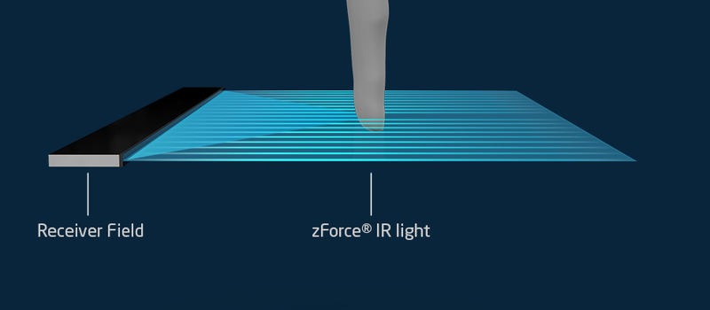
The display itself was a sort of focused Pepper’s Ghost illusion, reflected off of an expensive mirror made by Aska3D. I don’t know much more — I didn’t get to bring home one of the fancy glass plates — but it looked pretty good. But this display was interactive: you could touch the floating 2D projection as if it were actually there, and the software would respond. What was doing the touch response in mid-air? I’m a sucker for sensors, so I started asking questions and left with a small box of prototype Neonode zForce AIR sensor sticks to take apart.
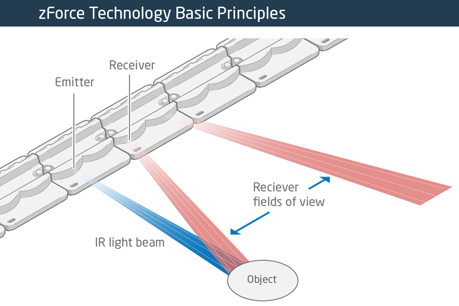 The zForce sensors are essentially an array of IR lasers and photodiodes with some lenses that limit their field of view. The IR light hits your finger and bounces back to the photodiodes on the bar. Because the photodiodes have a limited angle over which they respond, they can be used to triangulate the distance of the finger above the display. Scanning quickly among the IR lasers and noting which photodiodes receive a reflection can locate a few fingertips in a 2D space, which explained the interactive part of the floating display. With one of these sensors, you can add a 2D touch surface to anything. It’s like an invisible laser harp that can also sense distance.
The intended purpose is fingertip detection, and that’s what the firmware is good at, but it must also be the case that it could detect the shape of arbitrary (concave) objects within its range, and that was going to be my hack. I got 90% of the way there in one night, thanks to affordable tools and free software that every hardware hacker should have in their toolbox. So read on for the unfortunate destruction of nice hardware, a tour through some useful command-line hardware-hacking tools, and gratuitous creation of animations from sniffed SPI-like data pulled off of some test points.
Cracking Open the Case
In retrospect, it’s probably not necessary to take one of these things apart — the diagrams on the manufacturer’s website are very true to life. Inside, you’ll find a PCB with an IR laser and photodiode every 8 mm, some custom-molded plastic lenses, and a couple of chips. Still, here are the pretty pictures.


The lenses are neat, consisting of a 45-degree mirror that allows the PCB-mounted diodes to emit and receive out of the thickness of the bar. The lasers and photodiodes share lenses, reducing the manufacturing cost. Most of the thin PCB after the first three cells is “empty”, existing just to hold the laser and photodiode chips. It’s a nice piece of hardware.
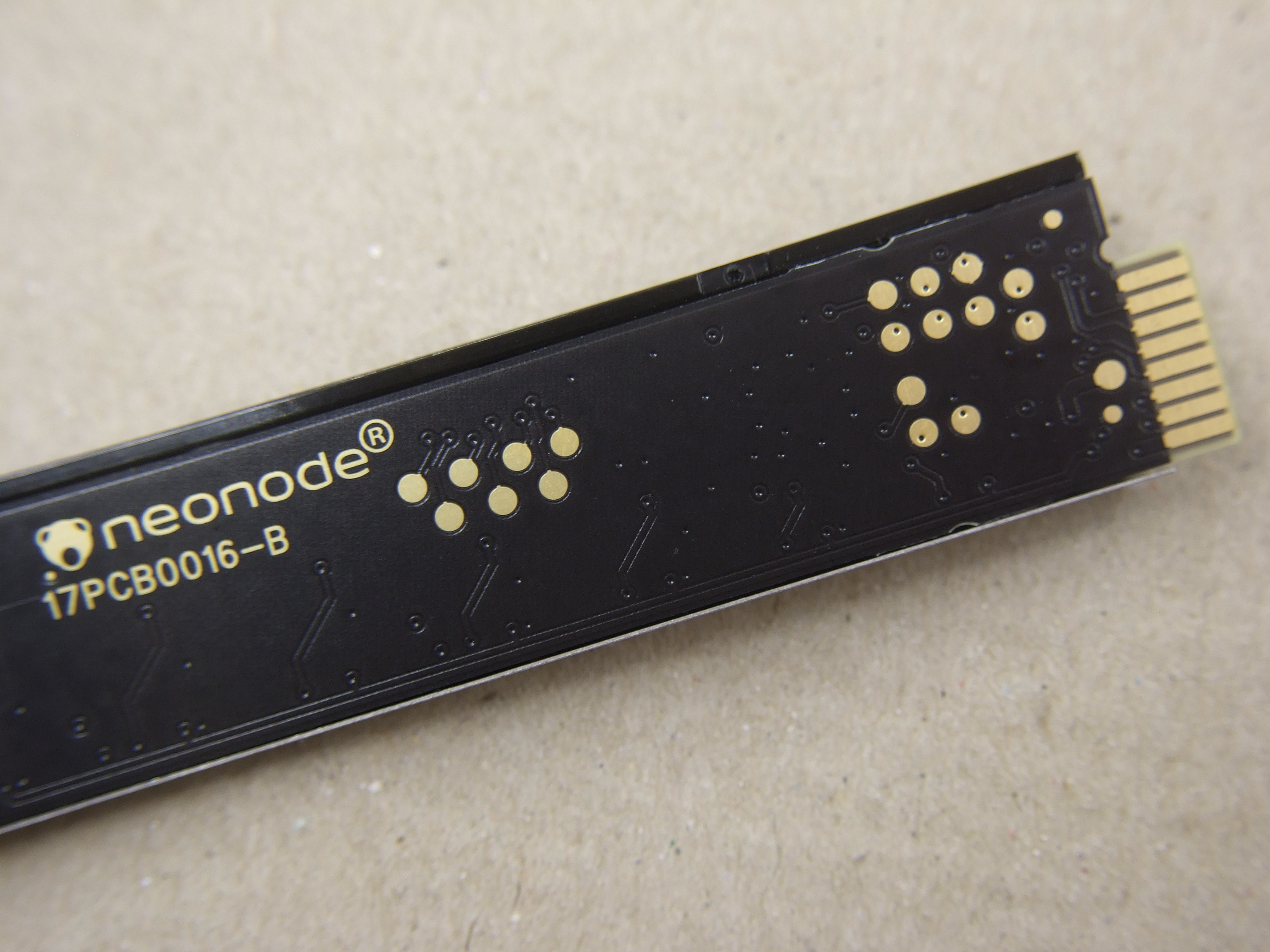
The chip-on-board ICs aren’t even covered in epoxy — although these boards are marked “prototype” so who knows if this is true of the production units. According to the advertising copy, one of these two chips is a custom ASIC that does the image processing in real-time and the other is a custom STM32 ARM microcontroller. Speculate about which is which in the comments!
The PCB is glued in place under the metal frame, and there are certainly no user-serviceable parts inside. Sadly, some bond wires got pulled loose when I was removing the PCB. When I put this one sensor stick back together, an area near the custom ASIC gets hot. Sacrificed for my idle curiosity! Sigh.
The Basics: The USB Interface
I was given a prototype version of the sensor demo kit, which includes a breakout board for the USB and I2C finger-detection functionalities of the sensors, so of course, I had to test them out. Plugging it in, and typing dmesg showed the “Neonode AirModule 30v” as a USB HID device, which means that figuring everything out about its USB functionality is going to be a cakewalk because all the data it spits out is described in a data descriptor.
I used usbhid-dump to read in the descriptor, and [Frank Zhao]’s excellent descriptor decoder to get it all in plain text. It looks like it’s a standard digitizer that supports six fingers and has a vendor-defined configuration endpoint. Here’s the descriptor dump if you want to play along. Dumps like this are great starting points if you’re making your own USB HID device, by the way. See what functionalities your mouse has.
 But frankly, pouring through a descriptor file is hard work.
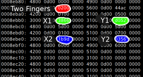
 dmesg said the sensor was attached as /dev/usb/hiddev3, so why not see what it’s doing in real-time while I wave my finger around? sudo cat /dev/usb/hiddev3 | xxd takes the raw binary output and passes it through xxd which turns it into a “human-readable” hexdump. (The genius of xxd is the -r flag which turns your edited hexdump back into a binary, enabling 1990’s-era cracking on the command line.) Just by watching the numbers change and moving my finger, I figured out which field represented the finger count, and which fields corresponded to the 16-bit X- and Y-coordinates of each finger. And it’s reporting zeroes for the un-measured fingers, as per the descriptor.
Of course, all of this, as well as the complete specs for the I2C interface are available in the zForce online documentation. The commands are wrapped up in ASN.1 format, which is a dubious convenience. Still, if all you want to do is use these devices to detect fingers over USB or I2C, it’s just a matter of reading some documentation and writing a driver.
Logic Analyzer vs. Test Points
 To have a little more fun with these sensor bars, I started poking around the test points exposed on the back of the unit. The set closest to the output connector are mostly duplicates of the pins on the connector itself, and aren’t that interesting. More fun are a constellation (Pleiades?) of seven test points that seem to only be available on the sensor bars that are longer than 180 mm.
One point had a clear 21 MHz clock signal running periodically, and two other lines had what seemed to be 10.5 MHz data, strongly suggesting some kind of synchronous serial lines. Two other pins in this area emitted pulses, probably relating to the start of a sensor sweep and the start of processed data, but that wouldn’t be obvious until I wired up some jumpers and connected a logic analyzer.
I really like the open-source Sigrok software for this kind of analysis. The GUI pulseview makes it fairly painless to explore signals that you don’t yet understand, while switching up to the command-line sigrok-cli for repetitive tasks makes some fairly sophisticated extensions easy. I’ll show you what I mean.
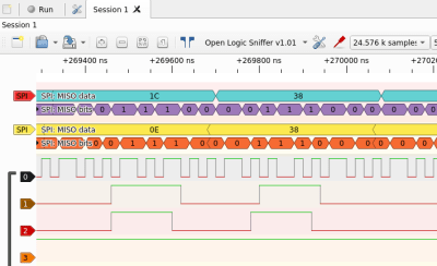
I started off with a Saleae Logic clone, based on the same Cypress FX2 chip. These are a great deal for $5 or so, and the decent memory depth and good Sigrok support makes up for the low 24 MHz sampling rate. That gave me a good overview of the signals and confirmed that the device goes into a low-power scan mode when no fingers are present, and that triggering when pin 5 went low isolated the bulk of the data nicely. But in order to actually extract whatever data was on the three synchronous serial pins, I needed to move up in speed.
The Openbench Logic Sniffer (OLS) will do 100 MHz, which is plenty for this application, but it has a very short 24 k sample memory that it has to relay back to Sigrok over a 115,200 baud serial line. Still, I could just squeeze a full read in at 50 MHz. Using Sigrok’s SPI decoders on the clock and two data lines gave me what looked like good data. But how to interpret it? What was it?
The Command Line, Graphics, and Real-Time Fingerwaving
Getting one capture out of pulseview is easy, but figuring out what that data means required building up a tiny toolchain. The command-line and sigrok-cli to the rescue:
sigrok-cli --driver=ols:conn=/dev/ttyACM3 --config samplerate=50m --samples 20k \
            --channels 0-5 --wait-trigger --triggers 5=0 -o capture.sr
This command reads from the OLS on the specified serial port, waiting for a trigger when channel 5 goes low and outputs the data in Sigrok’s (zipped) data format.
sigrok-cli -i capture.sr -P spi:clk=0:miso=1:cpha=1 -B spi | tail -c +3 > spi1.bin
sigrok-cli -i capture.sr -P spi:clk=0:miso=2:cpha=1 -B spi | tail -c +3 > spi2.bin
These two commands run the SPI decoders on the acquired data. It’s not necessary to do this in a separate step unless you’d like the output in two separate files, as I did. The -P flag specifies the protocol decoder, and -B tells it to output just the decoded data in binary. Tail aligns the data by dropping the three header bytes.
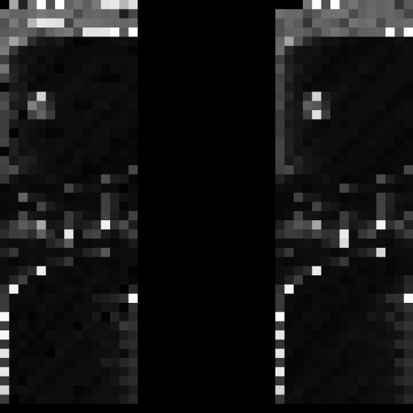
Now for the real trick: plotting the data, waving my finger around interactively, and hoping to figure out what’s going on. You’d be surprised how often this works with unknown signals.
t=`date +%s`
convert -depth 8 -size 15x45+0 gray:spi1.bin -scale 200 out1_${t}.png
convert -depth 8 -size 15x45+0 gray:spi2.bin -scale 200 out2_${t}.png
convert  out1_${t}.png spacer.png out2_${t}.png +append image_${t}.png
convert  out1_${t}.png spacer.png out2_${t}.png +append foo.png
 Convert
The two are then combined side-by-side (+append) with a spacer image between them, timestamped, and saved. An un-timestamped version is also written out so that I could watch progress live, using eog because it automatically reloads an image when it changes.
Cobbling all of this together yields a flow that takes the data in from the logic analyzer, decodes it into bytes, and turns the bytes into images. That was enough for me to see that I’m capturing approximate position data from (probably) the output of Neonode’s custom ASIC. But why stop there? I turned the whole endeavor into a video by combining the images at 8 FPS:
ffmpeg -r 8 -pattern_type glob -i "image_*.png" \
  -c:v libx264 -vf fps=8 -pix_fmt yuv420p finger_hand_movie.mp4
That’s me moving my finger just above the bar’s surface, and then out of range, and then moving one hand, and then both around in the frame. The frames with less data are what it does when nothing is detected — it lowers the scanning rate and apparently does less data processing. You can also see the reason for picking the strange width of 15 pixels in the images — there are 30 photodiodes in this bar, with data for 15 from one side apparently processed separately from the 15 on the other. Anyway, picking a width of 15 makes the images wrap around just right.
 There’s a bunch of data I still don’t understand. The contents of the header and the blob that appears halfway down the scan are still a mystery. For some reason, the “height” field on the bottom side of the data is reversed from the top side — up is to the right in the top half and the left in the lower half.
But even with just what I got from dumping SPI data and plotting it out, it’s pretty apparent that I’m getting the post-processed X/Y estimate data, and it has no problems describing the shapes of simple objects, at least like the flat palm of my hand. It’s a lot richer dataset than I got from just the default finger sensor output, so I’ll call the hack a success so far. Maybe I’ll put a pair of these in a small robot, or maybe I’ll just make a (no-)touch-pad for my laptop.
Regardless, I hope you had as much fun reading along as I did hacking on these things. If you’re not a command-line ninja, I hope that I showed you some of the power that you can have by simply combining a bunch of tools together, and if you are, what are some of your favorite undersung data analysis tools like these?


‘member neonode phones?
I `member LED-frame “touchscreens”. Hopefully this works better.
I’d rather learn what’s inside a neonode,
than learn a nematode’s inside me!
Neonode stock hasn’t done very well over the years.
Kind of what the Leap Motion™ did for hands.
The STM32 is the one on the left in the pictures (Chip A). It appears to be made with a finer lithography process, there’s a crystal oscillator circuit, and what appears to be the USB DP and DM signals, going through a couple of termination resistors, leading toward the card-edge connector.
Keep up the good work, Elliot!
You’re totally right! The USB pair is the dead giveaway.
Proper hack! Thanks Elliot!
But I want one (or more)! And they don’t sell them yet!
I checked just now and they have them in stock at Digikey. FWIW.
https://www.digikey.com/en/videos/n/neonode/introducing-the-zforce-air-touch-sensor
One of the most interesting articles in a while.
For I2C and SPI buses, Raspberry Pi and Python are the easiest way to peek and poke a device under the knife.
nice report on using sigrok-cli, I’m just getting into it myself. The idea of visualising the data is awesome! Will definitely come back for this later. Thanks!
I have some free zForce AIR samples at hand if someone like to build something cool, just drop me a line.
I also have some N2 phones in case there are someone with a desire to reinvent the past.
bengt.edlund@neonode.com
Nice hack. I have a 15 inch neonode and i want to hack it for a 12 inch screen. can I do that?