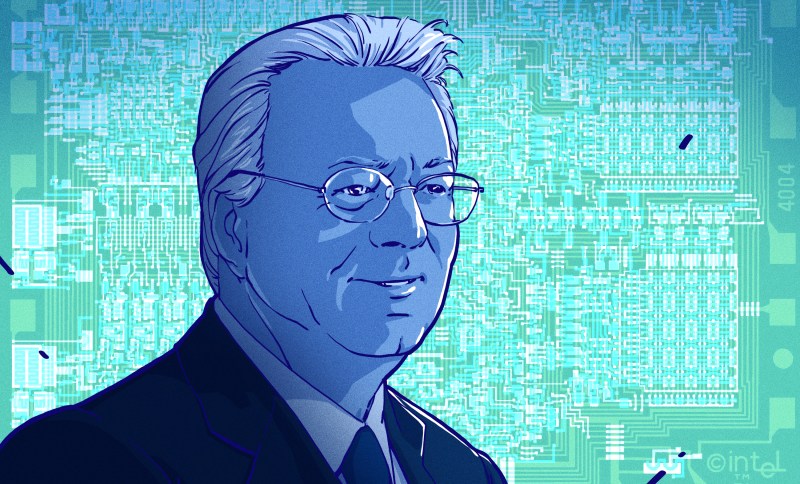
While doing research for our articles about inventing the integrated circuit, the calculator, and the microprocessor, one name kept popping which was new to me, Federico Faggin. Yet this was a name I should have known just as well as his famous contemporaries Kilby, Noyce, and Moore.
Faggin seems to have been at the heart of many of the early advances in microprocessors. He played a big part in the development of MOS processors during the transition from TTL to CMOS. He was co-creator of the first commercially available processor, the 4004, as well as the 8080. And he was a co-founder of Zilog, which brought out the much-loved Z80 CPU. From there he moved on to neural networking chips, image sensors, and is active today in the scientific study of consciousness. It’s time then that we had a closer look at a man who’s very core must surely be made of silicon.
Learning Electronics
Faggin was born in 1941 in Vicenza, Italy. From an early age, he formed an interest in technology, even attending a technical high school.
After graduating at age 19 in 1961, he got a short-term job at the Olivetti Electronics Laboratory. There he worked on a small experimental digital transistor computer with a 4096 word, 12-bit magnetic core memory and an approximately 1000 logic gate CPU. After his boss had a serious car accident, Faggin took over as project leader. The job was a great learning experience for his future career.
He next studied physics at the University of Padua where he graduated summa cum laude in 1965. He stayed on for a year teaching electronics to 3rd-year students.
Creating MOS Silicon Gate Technology (SGT) At Fairchild
In 1967 he started work at SGS-Fairchild, now STMicroelectronics, in Italy. There he developed their first MOS (metal-oxide-semiconductor) silicon gate technology (SGT) and their first two commercial MOS ICs. They then sent him to Silicon Valley in California to work at Fairchild Semiconductor in 1968.
During the 1960s, logic for ICs was largely done using TTL (Transistor-Transistor Logic). The two ‘T’s refer to using bipolar junction transistors for the logic followed by one or more transistors for the amplification. TTL was fast but took a lot of room, restricting how much could fit into an IC. TTL microprocessors also consumed a lot of power.
On the other hand, ICs containing MOSFETs had manufacturing problems that lead to inconsistent and variable speeds as well as lower speeds than was theoretically possible. If those problems could be solved then MOS would be a good substitute for TTL on ICs since more could be crammed into a smaller space. MOSFETs also required far less power.
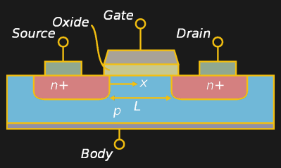
In the mid-1960s, to make an aluminum gate MOSFET, the source and drain regions would first be defined and doped, followed by the gate mask defining the thin-oxide region, and lastly the aluminum gate over the thin-oxide.
However, the gate mask would inevitably be misaligned in relation to the source and drain masks. The workaround for this misalignment was to make the thin-oxide region large enough to ensure that it overlapped both the source and drain. But this led to gate-to-source and gate-to-drain parasitic capacitance which was both large and variable and was the source of the speed problems.
Faggin and and the rest of his team at Fairchild worked on these problems between 1966 and 1968. Part of the solution was to define the gate electrode first and then use that as a mask to define the source and gate regions, minimizing the parasitic capacitances. This was called the self-aligned gate method. However, the process for making self-aligned gates raised issues with using aluminum for the gate electrode. This was solved by switching to amorphous silicon instead. This self-aligned gate solution had been worked on but not to the point where ICs could be manufactured for commercial purposes.
In 1968, Faggin was put in charge of developing Fairchild’s self-aligned gate MOS process technology. He first worked on a precision etching solution for the amorphous silicon gate and then created the process architecture and steps for fabricating the ICs. He also invented buried contacts, a technique which further increased the density through the use of an additional layer making direct ohmic connections between the polysilicon gate and the junctions.
These techniques became the basis of Fairchild’s silicon gate technology (SGT), which was widely used by industry from then on.
Faggin went on to make the first silicon-gate IC, the Fairchild 3708. This was a replacement for the 3705, a metal-gate IC implementing an 8-bit analog multiplexor with decoding logic and one which they had trouble making due to strict requirements. During its development, he further refined the process by using phosphorus gettering to soak up impurities and by substituting the vacuum-evaporated amorphous silicon with polycrystalline silicon applied using vapor-phase deposition.
The resulting SGT meant more components could fit on the IC than with TTL and power requirements were lower. It also gave a three to five times speed improvement over the previous MOS technology.
Making The First Microprocessors At Intel
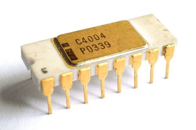
Faggin left Fairchild to join the two-year-old Intel in 1970 in order to do the chip design for the MCS-4 (Micro Computer System) project. The goal of the MCS-4 was to produce four chips, initially for use in a calculator.
One of those chips, the 4004, became the first commercially available microprocessor. The SGT which he’d developed at Fairchild allowed him to fit everything onto a single chip. You can read all the details of the steps and missteps toward that invention in our article all about it. Suffice it to say that he succeeded and by March 1971, all four-chips were fully functional.
Faggin’s design methodology was then used for all the early Intel microprocessors. That included the 8-bit 8008 introduced in 1972 and the 4040, an improved version of the 4004 in 1974, wherein Faggin took a supervisory role.
Meanwhile, Faggin and Masatoshi Shima, who also worked on the 4004, both developed the design for the 8080. It was released in 1974 and was the first high-performance 8-bit microprocessor.
Creating The Z80
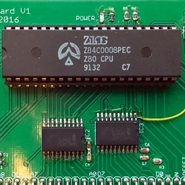 In 1974, Faggin left Intel to co-found Zilog with Ralph Ungermann to focus on making microprocessors. There he co-designed the Z80 with Shima, who joined him from Intel. The Z80 was software compatible with the 8080 but was faster and had double the number of registers and instructions.
The Z80 went on to be one of the most popular CPUs for home computers up until the mid-1980s, typically running the CP/M OS. Some notable computers were the Heathkit H89, the Osborne 1, the Kaypro series, a number of TRS-80s, and some of the Timex/Sinclair computers. The Commodore 128 used one alongside the 8502 for CP/M compatibility and a number of computers could use it as an add-on. My own experience with it was through the Dy4.
This is a CPU which no doubt many Hackaday readers will have fond memories of and still build computers around to this day, one such example being this Z80 Raspberry Pi look-alike.
The Z80, as well as the Z8 microcontroller conceived of by Faggin are still in production today.
The Serial Entrepreneur
After leaving Zilog, in 1984, Faggin created his second startup, Cygnet Technologies, Inc. There he conceived of the Communication CoSystem, a device which sat between a computer and a phone line and allowed transmission and receipt of both voice and data during the same session.
In 1986 he co-founded Synaptics along with Carver Mead and became CEO. Initially, they did R&D in artificial neural networks and in 1991, produced the I1000, the first single-chip optical character recognizer. In 1994 they introduced the touchpad, followed by early touchscreens.
Between 2003 and 2008, Faggin was president and CEO of Foveon where he redirected their business into image sensors.
Awards And Present Day
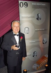
Faggin received many awards and prizes including the Marconi Prize, the Kyoto Prize for Advanced Technology, Fellow of the Computer History Museum, and the 2009 National Medal of Technology and Innovation given to him by President Barack Obama. In 1996 he was inducted into the National Inventor’s Hall of Fame for co-inventing the microprocessor.
In 2011 he and his wife founded the Federico and Elvia Faggin Foundation, a non-profit organization supporting research into consciousness through theoretical and experimental research, an interest he gained from his time at Synaptics. His work with the Foundation is now his full-time activity.
He still lives in Silicon Valley, California where he and his wife moved to from Italy in 1968. A fitting home for the silicon man.


Something that always puzzled me was… why did the Z80 use an 7-bit counter for the refresh counter, instead of 8 bits?
Parity? (8 bit with one parity only used in hardware)
some discussion:
https://retrocomputing.stackexchange.com/questions/5917/why-do-only-the-low-7-bits-of-the-r-register-increment
The last post by Jeremy seems the most plausible.
As Federico is still breathing, maybe an HaD staffer could ask him?
“In 2011 he and his wife founded the Federico and Elvia Faggin Foundation, a non-profit organization supporting research into consciousness through theoretical and experimental research, an interest he gained from his time at Synaptics. His work with the Foundation is now his full-time activity.”
That’s going to be quite the challenge.
Extreme challenge. I imagine that doing empirical, experimental research on consciousness is like drawing water from a stone. Somebody’s gotta do it.
We already did it in the moon… News today!
Z80 was a great chip. But I think Z8000 and Z80000 lacking compatibility with 8080/Z80 was a misstep for Zilog. Not that IBM would have selected it for the PC, but a series of CP/M-80 compatible systems extended to 16-bit and 32-bit could have competed against the PC as CP/M was effectively an open architecture. Might have let the later MSX stay alive longer too, especially the costs for a 16-bit variant kept going down.
The 8088 wasn’t backwards compatable with the 8080 either, so I don’t think that would have mattered. However IIRC IBM had done a project with the 8088 previously and had some familiarity with it
Correct, the pc was not IBM’s first experience with the 8088.
there was a standard tool from Intel that assembled 8080 mnemonics to 8086/8088. Porting old 8080 stuff to 8086 was easy, especially from CP/M-80 to CP/M-86, and to some degree DOS 2.x.
Z80 porting was harder because the tools were not as widely available, but even that translations famously occurred with in-house tools at Microsoft.
The 8086/8088 has a multiply instruction. The lack of multiply in the Z80 may have been critical. Zilog was slow to develop peripheral chips, in particular there was no reference design for expanding the addressing to 20 bits, as was done in the IBM PC.
A key, unmentioned, place for the Z80 is the TI graphing calculators (83, in particular). Still in there.
Not sure the best way to submit a tip, but in the last section Obama’s name is misspelled.
Fairchild, Intel, Zilog, Synaptics.. This guy led quite a busy career!
Thanks. Fixed.
I like how everything he worked on touched most of us: MOS, 8080, Z80, OCR, touchpads, touchscreens. Impressive!
This man is among the ‘royals’ of engineering.
Notice how must of us engineers think that we are building the future? We are not really doing anything of the sort. Very few people do anything of lasting impact. Consider some of my designs clever, but nothing that could not have been done by any other average engineer. At end of the day, will go home, pat the wife’s butt, and have an ale, after another long day of doing basically nothing of importance to humanity.
How is that for dismal, yet healthy and realistic perspective?
Sure the persons who developed Silly Putty or Crazy Glue felt the same way.
Most of us engineers are designing bridges and buildings and systems that improve people’s lives. That highway overpass doesn’t look like much, but many families get to spend a few more minutes together every day because it’s there. Every day, people fail to die in automobile accidents or medical malfunctions or household electrocutions because engineers are doing their jobs.
I like the phrase “every day, people fail to die”… like somewhere there’s a scooby-doo villain saying “I woulda gotten away with it too, if it weren’t for you meddlin’ engineers!”
Incredibly rare are people who do important work for humanity. It’s not just among engineers. I think the expectation that people should be doing such rare and important work on average is insanely over-optimistic and can only lead to anomie and depression. I think a lot of modern cultures today teach their kids that they can do anything and then expect them to actually be world-class, because why would they choose not to be? And that isn’t rational at all.
That reminds me of the person who caught Timothy McVeigh. A Highway Patrol officer that pulled over a speeder,
who turned out to have committed mass murder.
The problem with doing things that “build the future” is that you are responsible if it all goes wrong.
I don’t want blood on my hands.
I try to only make things that nobody dies if they fail.
Kind of the reverse of the Hackaday contest: “Make something that *doesn’t* matter!”
Good article,a genius who came through unusual beginings and also largely ignored in the story of the Microprocessor
Maybe Hackaday can put up a profile of Jerry Sanders, the founder of AMD, another ignored pioneer, one of my personal heroes.
Just looked him up. Yet another Fairchild Semiconductor alumi! And AMD was started by engineers who’d left Fairchild. Is there no end to the number of Fairchild employees who went on to do notable work?
Obviously the fact that half of Intel’s founders came from Fairchild as well should be noted!
in Intel’s rewriting of history Faggin doesn’t exist.
“The Commodore 128 used one alongside the 8502 ”
That should say “6502”
Great article! I’ve used the Z80 extensively but never knew of Faggin.
Thanks much. Fixed.
It actually is the 8502 which is an improved version of the 6510 which is a modified 6502. anyway you were right the first time.
Groan. I did check it before “fixing” it before but too fast I guess. The source has 8502 and 6502 in adjacent sentences. Fixed back. The webpage is getting a little worn where I keep erasing and rewriting but this should be the last time. :)
Thanks for the correction Bill and my apologies Steven.
I was working with the Z80, a lot, in the early 80s and a lot of my friends were also using the 6502.
I recall that the 6502 guys (who were also working on a hybrid Z80 + 6502 CP/M computer) were writing code for the C128 and Vic20, thus my mistake. Sorry for the headache!
did he do some work on the Performa 101??
You mean the Programma 101 but I do wonder if it influenced him deciding to go with designing a general purpose CPU vs a dedicated calculator on a chip for Busicom.
Hey HaD, how about tracing the lineage of the various micros like the 4004, Z80, 6502 etc.? Although they are considered obsolete, the core architecture & some peripherals still crop up in modern micros or get re-used across entire series of micros with lesser-known part numbers.
By way of example, TI have managed to re-use the TMS320 DSP for decades, shoe-horning it into ever more powerful SoCs, upping the clock speeds etc. but it’s basically an ancient design.
The Z80 fell out of favour in computers in the 1980’s but was still cropping up in industrial/commercial electronics 20 years later.
Yeah, great idea. Is there a modern version of each, that can maybe use the same software …
Well think of the 8051 for example it’s the core that drives the statemachine in every FTDI device of a certain generation. The cores are so well known that they are copied in to devices legitimately and otherwise. Sometimes good enough is just enough
Many SD cards also have a modified 8051 core, doing the write balancing etc. See this 30C3 video: https://www.youtube.com/watch?v=ruEn7TE4YMM (Bunnie Huang, Sean Cross)
The 65C02 still ships many units every year, less as DIP40s, more as soft cores.
It is amazing how HaD finds so many hidden geniuses who are the true sources of invention.
They should take a look at Isadore Biulkon (“The Siberian Monster”), the man who gave Tesla all his ideas and could actually do the math.
End of paragraph two, “who’s” should be “whose”
This is not an English class folks, and for my two cents worth the dude’s name is what really needs changed. Faggin, wow…
What I remember from working with him at CYGNET, he was soft spoken but approachable. I enjoyed the company and the people that worked there. Learned a lot right out of school, in hind sight he was way ahead of his time with the product. It launched my career in to the Internet world. Thank you sir!!!
I received an 8080 (S910) from that first batch, mentioned in Faggin’s book, Silicon. Worked from hand drawn data sheet/ timing diagram. S910 required -9VDC substrate bias. No software available. Reworked cross assembler(written in Algol) for 8008 to include 8080 instructions. Those were the days!
Some parts are a little misleading.
>”Faggin and and the rest of his team at Fairchild worked on these problems between 1966 and 1968″.
That sounds like it implies he invented all the techniques mentioned, but that is not true. Also, I don’t believe he was at SGS-Fairchild (Italy) when he invented the PolySilicon SGT ICs, it was Fairchild (US).
The real timeline for this tech and who invented it is as follows:
R.W. Bower (Hughes Aircraft, 1966) invented the self-aligned gate using Aluminum/Aluminium (aka. SAGFETs) not Faggin and team. They may have trialed and tested out Bower’s research themselves, but that is not how the article above reads. Worth noting that for Bower to get his Al-SAGs made, he relied on ion implantation (invented by Sprague Electric, 1965) due to heat issues from diffusion (higher temps) when Aluminum was used.
Independently Kerwin, Klein, Sarace (Bell Labs, 1966) invented self-aligned gates around the same time as Bower, but Bell used Amorphous Silicon rather than Aluminum/Aluminium. But these were discrete (due to lower mobility of charge carriers) amorphous Si SAGs, so were fairly limited in potential usefulness.
This is the point where Fairchild and Faggin step in (Fairchild 1968) took these other inventions but adapted processes by eventually inventing the use of polysilicon for the gate electrodes (with poly-Si having a much higher mobility) so that they could be used to create ICs (multiple MOSFETs in a single crystal of silicon). The FETs made with this approach were both SAGs and SGTs. But that wasn’t while at SGS Fairchild, that was in Fairchild (Silicon Valley) – for creating the 3708 SGT.
In his book, Silicon, Federico Fagin states that Intel received their first 8080 silicon in November of 1973. As an NDA customer, PCS received their first 8080 sample on 12/23/73 along with hand drawn timing diagram. We had both a wire wrapped and pcb boards ready for debugging at that time. By 01/04/74, the wire wrapped board was running and pcb artwork updated. On 01/14/74 we had the pcb running as well.
No real software was available, so we modified a cross assembler(written in Algol for the 8008) to include opcodes for the 8080.
Of the defects noted by Federico Fagin was a requirement for the substrate bias to be -9V instead of -5V and modified clock timing requirements.
Images of the CPU, processor and memory boards are available.
I still have original 8080 along with early versions by Mitel, TI & AMD.
Richard Barnich
K8bma.rick@ gmail.com