On the face of it, PCB production seems to pretty much have been reduced to practice. Hobbyists have been etching their own boards forever, and the custom PCB fabrication market is rich with vendors whose capabilities span the gamut from dead simple one-side through-hole boards to the finest pitch multilayer SMD boards imaginable.
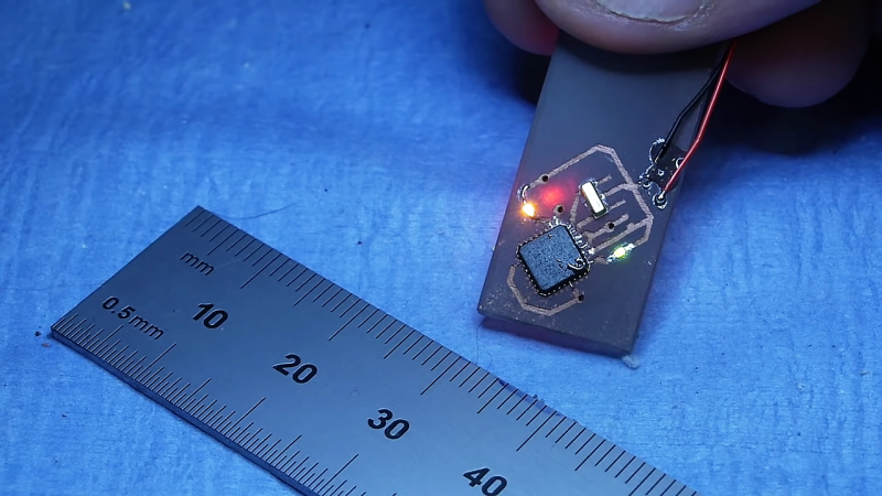
So why on Earth would we need yet another way to make PCBs? Because as [Ben Krasnow] points out, the ability to turn almost any plastic surface into a PCB can be really handy, and is not necessarily something the fab houses handle right now. The video below shows how [Ben] came up with his method, which went down a non-obvious path that was part chemistry experiment, part materials science. The basic idea is to use electroless copper plating, a method of depositing copper onto a substrate without using electrolysis.
This allows non-conductive substrates — [Ben] used small parts printed with a Formlabs SLA printer — to be plated with enough copper to form solderable traces. The chemistry involved in this is not trivial; there are catalysts and surfactants and saturated solutions of copper sulfate to manage. And even once he dialed that in, he had to figure out how to make traces and vias with a laser cutter. It was eventually successful, but it took a lot of work. Check out the video below to see how he got there, and where he plans to go next.
You’ve got to hand it to [Ben]; when he decides to explore something, he goes all in. We appreciate his dedication, whether he’s using candles to explore magnetohydrodynamics or making plasma with a high-speed jet of water.
Thanks for the heads up got to both [IraqiGeek] and [Victor].


That’s nuthin. Chemistry turns an egg into a chicken!
But where did the egg come from?
A more-reptilian thing
Wouldn’t it be the opposite? Who comes first?
Obviously the egg was first, since you first had egg laying creatures which slowly evolved into chickens, but since the eventual chicken came out of an egg, the egg came first.
Is an egg that produces a chicken, but isn’t laid by a chicken, a chicken egg? That’s the question and sounds an awful lot like a not-quite-like-a-chicken-egg, which means the resulting full chicken coming from that not-quite-egg came first.
For a simple metaphor, imagine boot-strapping a compiler.
To me the contents of the egg define the egg… so the first egg containing a chicken is the first chicken egg. Marshmallow eggs aren’t laid by marshmallows ;)
The most interesting thing I’ve learned today is that ‘marshmallow eggs’ exist.
Google shows me something similar to a marshmallow teacake.
Probably.
The rooster :D
Good post btw, with modern materials all sorts of options and worthwhile paths to explore…
Wow! Thanks for sharing this with the world. You are a true inventor – a lot of knowledge, then a lot of trial and error, and recording and reviewing results until you get to where you want to be. Keep going.
Ben always manages to amaze. He’s a tinkering rock star.
He’s a real-life mad scientist. He’s recreated more patents, equipment and experiments than any ten other engineers I know.
dude’s a freakin grand-master-wizard.
Yah, bit who’s on second?
I can think of two easier alternatives off the top of my head:
1. Get your pcb printed on thin transparent polymide and glue it to your plastic.
2. Prime your plastic with conductive paint, plate with copper, mask, etch, profit.
Not to belittle what he has done, but it’s sometime best not to reinvent the wheel.
Neither of your two suggestions as I comprehend them will allow you to make double sided “boards”. He has plated through vias from what I could see. And, he wouldn’t have to reinvent the wheel if the wheel weren’t shrouded in secrecy.
I apologize if my comment comes across as aggressive. I just don’t think you and he are on the same page with respect to why and what he did. I could be misreading your comment.
Have to agree completely. If it were not for people doing such things we would not progress.
I agree, the theory everyone knows; having the knowledge, patience and time few of us have. Being willing to share what you’ve learned is priceless.
Thank you. I think [Ben] deserves his own Hackaday prize!
I see where he’s coming from, the few pro plating forums around seem to exist to discourage and prevent anyone from plating anything. Had one guy going on a rant about what the EPA would do to me for pouring like an ounce of copper sulphate down the drain, when it was made up from about 2 teaspoons of root clear whose instructions were to pour the whole freaking 1lb package down there to remove roots. Yah dude, you guys aren’t allowed to dump 5000 gallons of it in the local river on a daily basis, I can dispose of a couple of ounces once in a blue moon without getting licensed by your bullshit professional organisation and the EPA etc.
Oh yeah and the patent crap, many electrochemistry patents you get this compound, and/or this one, and/or this one, with this one and/or this one and/or this one, with concentrations ranging from 1-70% at a temperature of from 200 to 400 Kelvin and/or and/or and/or … that’s not full disclosure, that’s a shotgun patent, and 90% of those million combinations probably actually do nothing, with a very tight range of commercially effective compounds and concentrations, they ought to be thrown out and only working and fully disclosed specific formulas given the benefits of patent protection.
1) wouldn’t work very well on surfaces with compound curves.
2) would quickly get impractical to plate as the number of disjoint traces rise.
I love Pcb designing.
Guess the last minute of this video is the most interesting one. If he found basically working copper traces just by accident, there’s certainly a way to reliably take advantage of it.
That looks basically like what the industry calls 3D MID (Molded Interconnect Devices). There are some neat examples on the web, but outside of RF-antennas in smartphones, i’ve never seen any product that actually uses the technology to gain a significant advantage.
oh! Interesting concept
Copper oxide in epoxy as a paint, lazer that for an electrodeless plate?
Hmm, so are you writing Erik Johnson that the carbon in the epoxy when lasered with reduce the CuO to Cu ?
Then bond well enough to the substrate, seems reasonable though the formulation of CuOepoxy mix would need assessment for such things as; retention, resistivity, RFI impedance issues, current capacity, discharge of products of reduction such as volatiles during lasering etc.
With some 20,000 plus epoxy options its not a trvial exercise to explore even 5% of that, though a plausible line of enquiry for a turn-key system where client often makes short run prototypes and needs results on the day and then best where closest to properties of a production board…
I am writing, Mike Massen, to wonder if the last experiment in the video showing the laser etching sintering the Cu out of the resin could work as the base for the Cu solution to drop on to in lieu of performing the Pd steps.