3D Printer Emission Monitor Quantifies The Stench

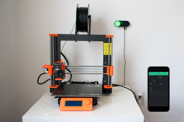
While we don’t yet know the long-term effects of hanging out around 3D printers, it doesn’t take a in-depth study to figure out that their emissions aren’t healthy. What smells toxic usually is toxic. Still, it’s oh-so-fun to linger and watch prints grow into existence, even when we have hundreds or thousands of hours of printing under our belts.

Most of us would agree that ABS stinks worse than PLA, and that’s probably because it releases formaldehyde when melted. PLA could be viewed as slightly less harmful because it has a lower melting point, and more volatile organic compounds (VOCs) are released at higher temperatures. Though we should probably always open a window when printing, human nature is a strong force. We need something to save us from our stubbornness, and [Gary Peng] has the answer: a smart 3D printer emission monitor.

The monitor continually checks the air quality and collects data about VOC emissions. As the VOCs become elevated during printing, the user is notified with visual, audio, and phone notifications. Green means you’re good, yellow means open a window, red means GTFO. There’s a brief demo after the break that also shows the phone interface.

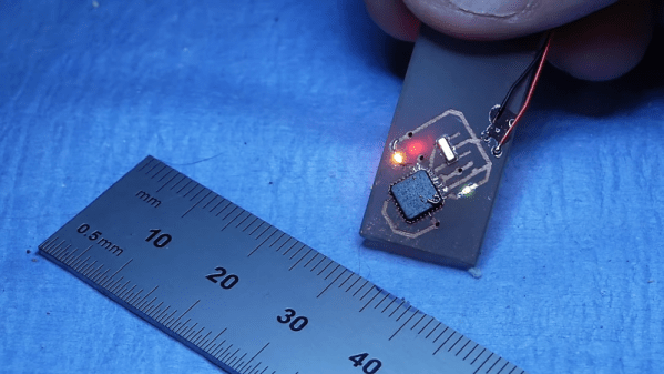
The heart of this monitor is a CCS811 gas sensor, which provides VOC data to a Particle Photon. [Gary] built a simple Blynk interface to handle the alerts and graph historical VOC readings. He’s got the code and STLs available, so let this be the last time you watch something print in blissful semi-ignorance.

Concerned about air quality in general? Here’s a standalone portable monitor designed to quantify the soul-crushing stuffiness of meetings.

Continue reading “3D Printer Emission Monitor Quantifies The Stench”

Chemistry And Lasers Turn Any Plastic Surface Into A PCB

On the face of it, PCB production seems to pretty much have been reduced to practice. Hobbyists have been etching their own boards forever, and the custom PCB fabrication market is rich with vendors whose capabilities span the gamut from dead simple one-side through-hole boards to the finest pitch multilayer SMD boards imaginable.

So why on Earth would we need yet another way to make PCBs? Because as [Ben Krasnow] points out, the ability to turn almost any plastic surface into a PCB can be really handy, and is not necessarily something the fab houses handle right now. The video below shows how [Ben] came up with his method, which went down a non-obvious path that was part chemistry experiment, part materials science. The basic idea is to use electroless copper plating, a method of depositing copper onto a substrate without using electrolysis.

This allows non-conductive substrates — [Ben] used small parts printed with a Formlabs SLA printer — to be plated with enough copper to form solderable traces. The chemistry involved in this is not trivial; there are catalysts and surfactants and saturated solutions of copper sulfate to manage. And even once he dialed that in, he had to figure out how to make traces and vias with a laser cutter. It was eventually successful, but it took a lot of work. Check out the video below to see how he got there, and where he plans to go next.

You’ve got to hand it to [Ben]; when he decides to explore something, he goes all in. We appreciate his dedication, whether he’s using candles to explore magnetohydrodynamics or making plasma with a high-speed jet of water.

Continue reading “Chemistry And Lasers Turn Any Plastic Surface Into A PCB”