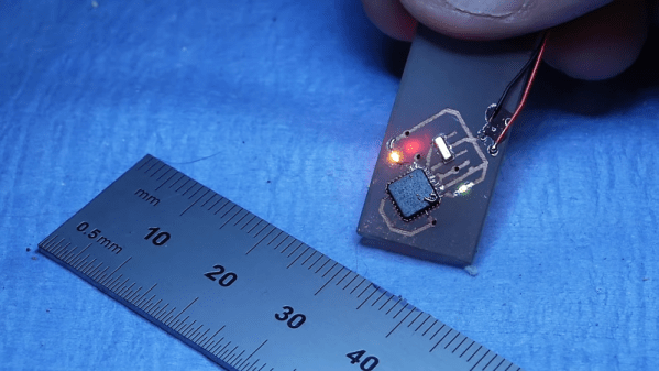
There are plenty of chemical processes that happen commonly around the house that, if we’re really following safety protocols to the letter, should be done in a fume hood. Most of us will have had that experience with soldering various electronics, especially if we’re not exactly sure where the solder came from or how old it is. For [John]’s electroless plating process, though, he definitely can’t straddle that line and went about building a fume hood to vent some of the more harmful gasses out of a window.
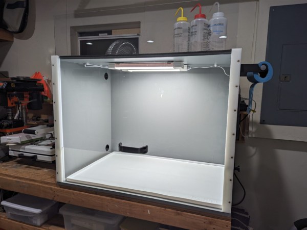
This fume hood is pretty straightforward and doesn’t have a few of the bells and whistles found in commercial offerings, but this process doesn’t really require things like scrubbing or filtering the exhaust air so he opted to omit these pricier and more elaborate options. What it does have, though, is an adjustable-height sash, a small form factor that allows it to easily move around his shop, and a waterproof, spill-collecting area in the bottom. The enclosure is built with plywood, allowing for openings for an air inlet, the exhaust ducting, and a cable pass-through, and then finished with a heavy-duty paint. He also included built-in lighting and when complete, looks indistinguishable from something we might buy from a lab equipment supplier.
While [John] does admit that the exhaust fan isn’t anything special and might need to be replaced more often than if he had gone with one that was corrosion-resistant, he’s decided that the cost of this maintenance doesn’t outweigh the cost of a specialized fan. He also notes it’s not fire- or bomb-proof, but nothing he’s doing is prone to thermal anomalies of that sort. For fume hoods of all sorts, we might also recommend adding some automation to them so they are used any time they’re needed.
Continue reading “Custom Fume Hood For Safe Electroless Plating”