Understanding the nature of pH has bedeviled beginning (and not-so-beginning) chemistry students for nearly as long as chemistry has had students. It all seems so arbitrary, being the base-10 log of the inverse of hydrogen ion concentration and with a measurement range of 0 to 14. Add to that the electrochemical reactions needed to measure pH electronically, and it’s enough to make your head spin.
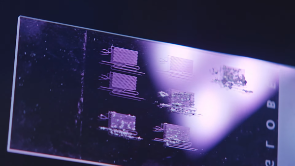
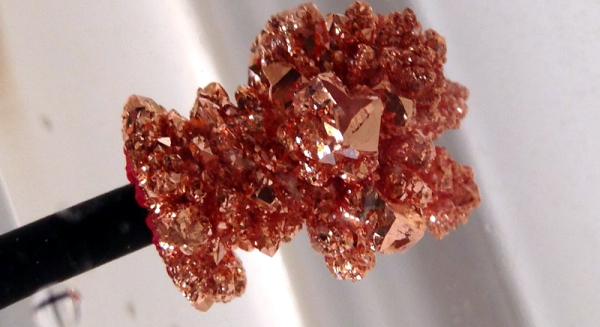
Difficulties aside, [Markus Bindhammer] decided to tackle the topic and came up with this interesting digital pH meter as a result. Measuring pH electronically is all about the electrode, or rather a pair of electrodes, one of which is a reference electrode. The potential difference between the electrodes when dipped into the solution under test correlates to the pH of the solution. [Markus] created his electrode by drawing molten antimony into a length of borosilicate glass tubing containing a solid copper wire as a terminal. The reference electrode was made from another piece of glass tubing, also with a copper terminal but filled with a saturated solution of copper(II) sulfate and plugged with a wooden skewer soaked in potassium nitrate.
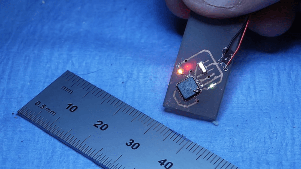
In theory, this electrode system should result in a linear correlation between the pH of the test solution and the potential difference between the electrodes, easily measured with a multimeter. [Marb]’s results were a little different, though, leading him to use a microcontroller to scale the electrode output and display the pH on an OLED.
The relaxing video below shows the build process and more detail on the electrochemistry involved. It might be worth getting your head around this, since liquid metal batteries based on antimony are becoming a thing.
Continue reading “Homebrew PH Meter Uses Antimony Electrode”