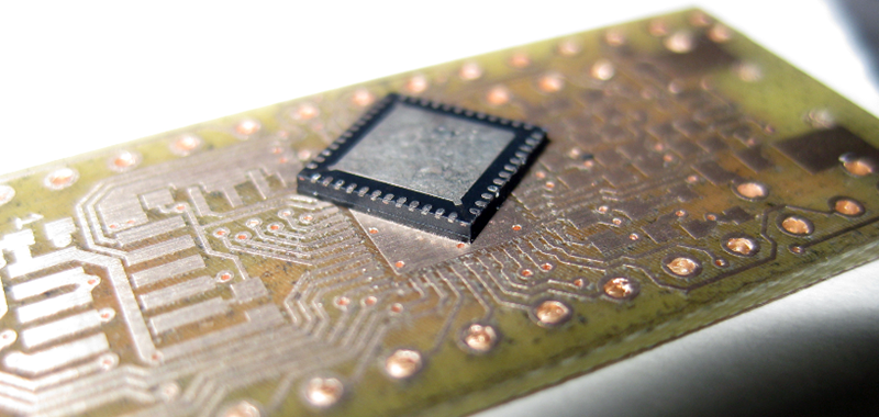
Every once in a while, you’ll find some weirdness that will send your head spinning. Most of the time you’ll chalk it up to a bad solder joint, some bad code, or just your own failings. This time it’s different. This is a story of weirdness that’s due entirely to a pin that shouldn’t be there. This is a package for an integrated circuit that has a pin zero.
The story begins with [Erich] building a few development boards for the Freescale Kinetis K20 FPGA. This is a USB-enabled microcontroller, and by all accounts, a worthwhile effort. So far, so good. The problem with the prototype boards was soon apparent. On some of the boards, the external 32 kHz oscillator was not starting. Resoldering the oscillator or microcontroller sometimes solved the problem, but not always. This is troubling, because that means the issue isn’t code, and it’s not the PCB. This is going to take a deep dive and a good inspection microscope.
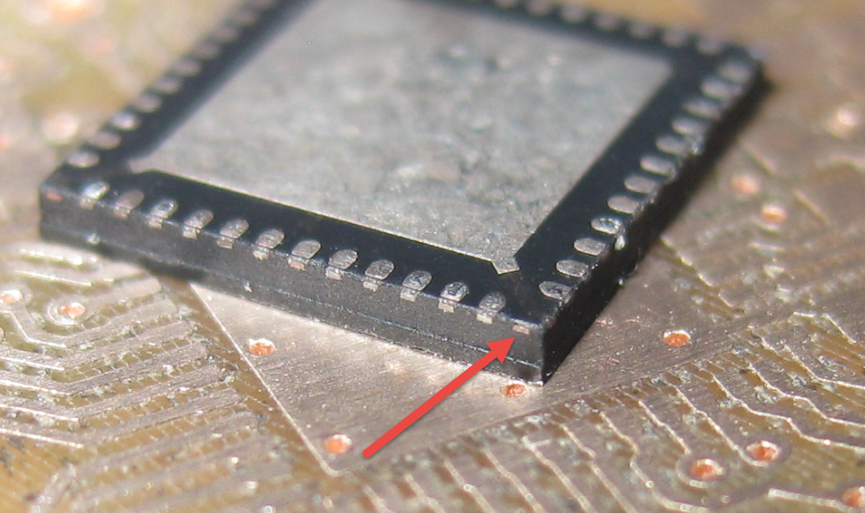 One of [Erich]’s friends, [Christian B] somehow found the problem. When the Freescale K40 is manufactured, the die is carefully laid in a chip carrier and coated with epoxy, putting it in a small QFN package. The problem is, there’s an extra connection sticking out of one corner of this chip. This is just an artifact of the chip carrier, but if you leave exposed metal connected to ground, something is eventually going to go wrong.
The best guess [Erich] has is that this additional connection is from the manufacturing and packaging process, with the exposed metal pad in this application being bridged to an adjacent pad. Now, if there’s one failure to [Erich]’s design, it’s that the trace comes out of the pin on the adjacent pad at 90 degrees; this isn’t a best practice, but most of the time you can get away with it. This time, though, somebody got burned.
We don’t know how [Christian] ever found this issue. When you look at a tiny QFN package, you don’t expect there to be an extra pin attached to ground that can be easily bridged with a bit of solder paste. It’s either a lot of luck or skill to find this problem, but it’s a great example of the weird things you have to look out for.


Annoying! Thankfully someone found this problem.
K20 or K40? The text says both.
And they’re both ARM microcontrollers, not FPGAs.
There are often little vestiges of the leadframe like this, especially on leadless packages. Sometimes they’re called out on drawings, sometimes not. Bummer that it caused a problem for this person, but in this case it looks like using a maskless PCB was a big part of the problem
I’ve been seeing these little titties all of my life on IC’s. I’ve just never thought of them till now, now that you made a point of showing them. If I have time today I will go thew some of my IC Boxes and see if I can give some number of the chips that has them on them.
Thanks
I wouldn’t count on solder mask fixing the problem in the long term.
Really? How long a term are we talking about?
At least somebody got the terminology correct. it is a “leadframe” no a chip carrier, and yes, they can be conductive to silicon for various reasons.
I spotted this at work and thought if I ever had to fix a trace running under those “hidden pins”, just how much hassle would be caused by those tabs?
My guess is confirmed here, so I’ll probably write off said boards instead. Luckily I’ve not seen my hypothetical situation actually occur yet at work.
…and all of that could be prevented by always exiting the pads straight and not on the side. It’s the same with 45° bends or other “optional” PCB rules like vias in pads.
Is it always necessary? No
Does it help in some cases? Yes
Does it look good? Yes
Yes, you are absolutely right. Making electronics is some kind of art with own rules. And they are good for you to follow them.
Sounds like best practice for this part would be to put a little isolated pad in that spot. If it solders to it, it provides a little extra mechanical support. If it doesn’t solder to it, no harm.
Nice suggestion.
Every PCB trace is an antenna. In theory, it can still cause unexpected things to happen if on some board it is soldered to it and on other boards not.
This is rather typical that there is remnants of the lead frame, unless the Center pad that holds the chip also happens to be connected to some of the actual pins on the package, then there is potential for no such hidden pins.
But I myself follow the rule that SMD components will always have some trick up their sleeve to make my life harder… Be it tiny solder bridges, or hidden pins, or a solder bridge from a leadless pin to the center pad, something one hardly can even see….
repost of this
https://hackaday.com/2015/10/13/fail-of-the-week-marginally-documented-pad-shorts-to-maskless-pcb/
At least that last title was precise and accurate, not like this “epoxy is conductive” BS
You don’t mount your Freescale FPGAs with conductive epoxy?
@walter – Agreed – the title was misleading and confusing. Read it twice… still not sure how ‘conductive epoxy’ applies here.
And the other article was better, it showed exactly how and where the design was flawed, looks like an easy mistake to make though,
Doh! Sorry about that.
Some of our readers missed it the first time around, judging by the comments, so maybe it was an (unintentional) public service. :)
I think this article resurfaced on reddit , and then someone tipped HaD about this. But those guys still should have gone thought comments on the original article , as it says that there was a post on Hackaday about this article
No, it’s a trick title. The fail of the week is this post itself!
Misleading and clickbaiting title: the epoxy is no way conductive.
And as mentioned, on a normal (solder masked) PCB, there is no way to have any issue with this extra pad.
Repost of this
https://hackaday.com/2018/11/18/fail-of-the-week-when-the-epoxy-coated-chip-is-conductive/#comment-5476175
Repost of this
https://hackaday.com/2018/11/18/fail-of-the-week-when-the-epoxy-coated-chip-is-conductive/
Sorry mods, not spamming. My mistake.
not sure why, but for some reason i half expected the epoxy to be the culprit
You’re Not alone, I imagined a populated pcb waterproofed with (conductive) epoxy resin, not an unused spare pin poking out of a package.
Well that certainly wouldn’t work very well lol
That’s a good example why it is better to invest in solder mask. I consider a SMD design without solder mask to be a hack ;)
BTW: For DIY etched layouts you can use solder mask repair pens to coat at least the more important areas like fine pitch IC pads etc.
You had me with “solder mask repair pen”!
I don’t have one, but I use fingernail polish or carefully cut electrical tape for the same purpose. Like the time I let the ground plane pour run through the middle of one of those 868 MHz radio modules…
There have been several comments saying that solder mask would solve the problem. I have always assumed that solder mask could eventually wear through if there was vibration. In this case, the chip is pretty solidly attached to the board, so that’s less of a problem.
Am I being too cautious?
The solder mask is not so much used for (permanent) isolation. In fact in my business, we are not allowed to rely on the isolating properties of the solder mask at all. The more important property is that prevents the flow of solder into areas where it could cause problems during assembly.
Another thing that can help allot is the use or a flux pen. If you see that you got bridges, add some of the flux and remelt the joint. The additional flux dissolves oxidation layers on the liquid solder which helps to break these bridges.
I don’t think the “pin” was in mechanical contact, but just close enough that the solder could surface-tension itself into a bridge. And that’s exactly what soldermask is for.
Yes, you’re being too cautious. I have never seen vibration wear through solder mask on a properly soldered component and I’ve looked at thousands of failed boards. I have seen:
– Improperly etched boards leaving copper “tails” that short between tracks and pads.
– Poorly cleaned boards (from the fabrication stages ) become conductive under the solder mask.
– Poorly cleaned boards responsible for the solder mask flaking off.
– Metal bridges grow between pins, pads and tracks due to operation in high humidity ( electrochemical migration ).
– Even a fingerprint kill a clock circuit because the operator was eating potato chips on the production line.
” I have never seen vibration wear through solder mask on a properly soldered component…”
Have oft seen it. But should qualify that – I do a HALT series on my employer’s during design phase and a short regression on products before release to production. And this stuff meets IPC600/6 and IPC222x.
Never seen vibration-related failure either personally, but then again, none of my PCBs are in an environment prone to vibration stress. I have received boards that had insufficient/uneven masking, resulting in solder shorts after they were solder waved.
If you look closely at the chip, that “pin zero” (a remnant of the leadframe) is actually a short distance up the side of the package and wouldn’t be directly in contact with the PCB. It doesn’t continue along the bottom of the package like the normal pins do. What happened was some solder paste was bridging the tiny distance and soldering it to a nearby 90-degree trace in the reflow oven. Which is exactly what a solder mask is intended to prevent.
Even if the mask did wear off later (which is doubtful) it wouldn’t cause a short unless it was soldered again. A mask would have worked fine.
The Juno 106 VCOs suffer a similar problem.
That’s actually a common internet misconception about the Juno I’d like to dispel. It is not the epoxy being conductive, but the epoxy that gets under the ICs and pops them off the board when thermal expansion and contraction occurs with usage. I’ve fixed over a thousand 106s and I tested dozens for conductivity and capacitance and not once has any batch had any significant reading. It’s just the fact it’s one of the first examples of SMD construction in a consumer product, and they didn’t do enough rigorous testing at Sharp (the manufacturer of the 80017) of the mechanical properties of the custom Roland BA662/IR3109 VCA/VCF ICs they encapsulated. Non-conductive epoxy is non-conductive :D
I use the same Freescale K2X part in this same package in several different designs and I have yet to have this issue…That being said I do find that I have to be more attentive to the stencil aperatures and solder paste application, as one can get a bulbous solder blob during reflow.
ya, this is what happens when you dont spend the extra $0.02 to get a solder mask on your PCB, and dont apply solder paste properly. There is no way that edge pin would stick to anything with a solder mask, and if there was no solder paste below it.
So typical from NXP! Once upon a time I was designing my first all SMD board, very extensive (510 components) and I have most issues with LQFP208 package… NXP has a lot of errata on datasheets and manuals, and in this case, some incomaptibilities not documented for 208 packaage!!!
Back in ancient history (1979) when I was a newbee EE at a pacemaker company we had production line yield issues that were caused by ink marks made by inspectors. The circuit was a CMOS NAND gate configured to be an oscillator (72 beats per minute). The ink they were using was conductive and changed the R in the RC oscillator. I got to be a hero my first week on the job.
Many years ago I had to analyze DRAM chips that were failing due to low impedance between a couple of adjacent pins. These pins spent the majority of the time at opposite voltages (back in the old days – the ‘80s – when DRAM chips used multiple supply voltages), and enough contaminants from mildly active flux were getting into the chip to dissolve some silver from the leadframe plating. Potential difference between the affected pins was more than enough to cause silver dendrites (fingers) to plate out along pores in the epoxy. In a few cases we could even see the silver dendrites under a light microscope, though we originally “saw” the dendrites using a scanning electron microscope.
Now THAT was conductive epoxy causing chips to fail!
I experienced the same thing with SHARP proximity sensors couple of days ago…
Anyone have a list of chips that have this “feature” I oddly remember it on a Spartan or Xilinx chip. Please correct me.
Had this happen to me once, and it was not this part put another that I can not remember…
This is common to many QFN components. Got a batch of SiFive FE310 in front of me that have the same quirk.
On a board with no soldermask, why not put a tiny bit of kapton tape on just that exact spot where this pin 0 solders to?
(Also: where is the conductive epoxy? Title is misleading.)