It is getting so easy to order a finished printed circuit board that it is tough to justify building your own. But sometimes you really need a board right now. Or maybe you need a lot of fast iterations so you can’t wait for the postal service. [Thomas Sanladerer] shows how he makes PCBs with a CNC machine and has a lot of good advice in the video below.
He starts with Eagle, although, you could use any creation package. He shows what parameters he changes to make sure the traces don’t get eaten away and how to do the CAM job to get the files required to make the boards. If you don’t use Eagle, you’ll need to infer how to do similar changes and get the same kind of output.
We’ve only heard a few people pronounce Gerber (as in Gerber file) with a soft G sound, but we still knew what he meant. We have the same problem with GIF files. However, once you have Gebers, you can join the video’s workflow about 5 minutes in.
At that point, he uses FlatCAM to convert the Gerbers to a single G-code file that integrates the paths and drill files. There were a few tricks he used to make sure all the tracks are picked up. Other tricks include leveling a spoil board by just milling it down and mounting different size bits. He also has ideas on aligning the Z axis.
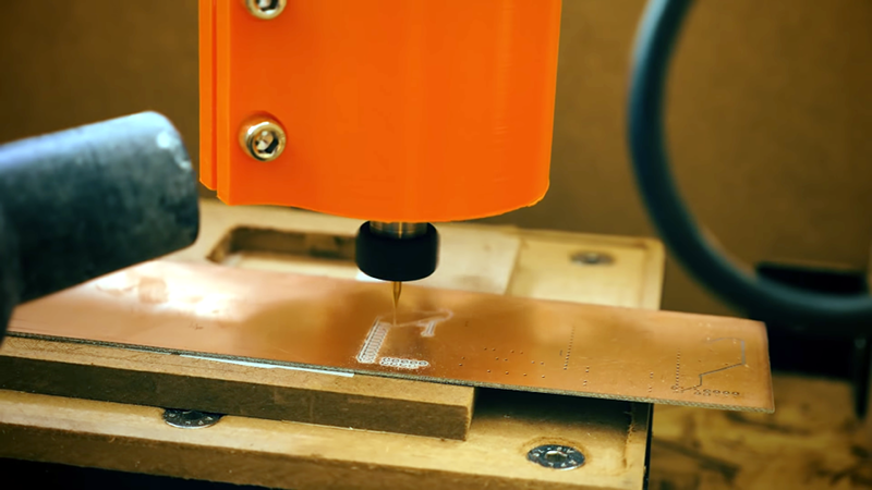
He first did a mock-up with some MDF scrap. The final boards, of course, use copper clad FR-4. Interestingly, the mock-up served as a position guide for the board. Even if you didn’t do an entire mockup, milling the profile of the board might be a good idea. Naturally, the first attempt wasn’t great and he aborted it. He simplified the board layout and tried again but that didn’t work well. He then switched out the engraving bit he was using for a proper end mill. That caused a bit of an edge that needed sanding, but solved most of the other problems.
It looks like for simple boards, the technique works ok, although there were some limitations. Some of the traces were the wrong width and some annuli didn’t survive the drilling. It also appears it isn’t reliable to place traces between IC pads using this milling process.
We’ve avoided some of the problems [Thomas] had by auto-levelling the FlatCAM output. We’ve also seen milling used to just remove resist followed by a traditional acid etch, which gives good results.


I use my laser engraver to burn off spray paint masking… works well! (also etched the board in this video using Vinegar and Peroxide rather than much harsher and dangerous etchants like FeCl..
https://www.youtube.com/watch?v=657Jg0fUbvk
It’s so DANGEROUS that they would use in water treatment.
https://en.wikipedia.org/wiki/Iron(III)_chloride#Industrial
It’s not dangerous (well, you should not eat it) but it makes a horrible mess and nasty spots(??) on clothing.
So is chlorine, but I wouldn’t recommend drinking concentrated bleach.
Once you etch a bunch of copper with it, it’s no longer ferric chloride. Now it’s cupric chloride, which is a hazardous waste that’s illegal to put it down your drain; you must dispose of it properly.
this is interesting . ta for sharing
im wondering : if you can register the board well enough back in the laser cutter, you may be able to remove paint from the pads only leaving the paint on the traces as a poor mans solder resist
I have done a bit of both laser and CNC at home and I definitely prefer the laser method. Nicer results and less worry about cancer causing fiberglass dust.
I think double sided is easier with a cnc. Dust extraction deals with the, er, dust. And no nasty copper infused chemicals to dispose of.
Use FR2 (“Pertinax”), the brown stuff without glass inside. Harder to get these days, but much better suited. Doesn’t dull milling bits like no tomorrow.
Also, covering the entire board in water during milling is a good idea. Zero dust.
See https://vimeo.com/28673339 and https://reprap.org/wiki/Mantis_Electron
Definitely this — you can even easily buy cheap FR-1 blanks from the likes of Bantam Tools: https://www.bantamtools.com/collections/materials/products/pcb
For those with a Smoothieboard note you can do this directly with the board itself, using either a probe, or simply the crocodile-clip+contact method : http://smoothieware.org/zprobe
For a single board, FR-4 is fine, but if you value your health and the life of your bits, use FR-1 or FR-2 – they’re resin or resin bonded paper, instead of fiberglass in epoxy. The glass dust is a bit nasty.
I had a question about the CNC milling: I’m guessing that the bed really needs to be leveled manually, and not using an “automatic” leveling routine with a contact sensor of some kind that adjusts the z axis based on the measured offsets, since that may lead to too much variance in the depth of cut on a thin PC board. Or am I overly cautious?
On CNCs you typically level your bed by machining it ( typically using a “surfacing” operation that ensures the bed is then perfectly level with the spindle/axes ).
Sorry about my comment, I think I understood him comment as talking about CNC milling in general, so I answered about surfacing, but obviously that’s completely irrelevant when talking about machining PCBs, you can’t do surfacing there ( or can you ? I’d be curious to know if it’s possible or ever makes sense. Maybe if the pcb is very flat already, and the copper is pretty thick, a surfacing pass might make sense ? )
its not do much about the bed. the fiberglass has inconsistent thickness, varying .010″ at times. when making a .003″ cut it creates incomplete cuts or too much cut depth. autolevel maps the true height of the piece to be cut, the applies the difference the the z axis, boards come out very nice. opencncpilot is a nice grbl dender with autolevel, along with bcnc and chillipepper, there are also options for mach3.
Not only do the have varying thickness, the boards you cut out from larger sheets inevitably have a bend or twist in them, and they’re mighty difficult to keep flat on the bed. If you double-side tape them, they’ll peel or bow off slightly.
Oh, you can definitely autolevel a PCB much more easily than anything non-conductive. Both BCNC and Chilipeppr have functionality allowing you to use a special gcode command (available in at least grbl) that’ll stop the bit once a circuit is made — so you clip one side of a circuit to your drill, and one side to the PCB itself, and probe at multiple points along the board to build a mesh. It works pretty flawlessly.
Yes the Gcode you are looking for is G30 : http://smoothieware.org/G30 . Smoothie also supports the XY version of that ( I think it might be G38 ) which is very nice to find the corner of a workpiece with the appropriate sensor ( or via the contact/circuit-closing method if working metal ).
I find G30 for Z part finding, and for XY corner finding, is one of those techniques that lots of people put off learning/implementing on their machines, but once they finally stop procrastinating, it’s nearly universal how people love it and wonder how they could have lived without it.
with a spring loaded spindle it is rather simple to engrave stuff with uneven surfaces: http://www.2linc.com/images/engraved_cnc_milling.jpg
This will be very useful when the United States goes to war with China and we can no longer order cheap PCBs. Always good to have a backup plan!
And then China will be stuck forever with LAST YEAR’S IPHONE.
Is there a way to make vias?
The easiest way would be to make two pads in the same location on the board on both sides. Drill the through hole and connect by soldering on both sides of board.
What are the limitations of CNCs like 3018-PROVer over smaller footprints like FPC or Hirose connectors or very small SMD microchips which have a very small spacing between pins. I’ve searched on the CNC specs to see what is the minimum motor step to check it can move at the desired precision but I can’t find such information. Is it only dependent on the drill bit diameter?
The smallest footprint I’ve been able to mill on my PROVer v2 is TDFN-8, with trace widths of approximately 0.15mm. Issues with variable trace widths can be solved by using micro 2 flute flat end mills. The biggest problem you’ll have though is burring and the need for multiple depth cuts to keep vibration to a minimum. Then you have the problem of solder resist removal. Even with a spring loaded end-mill if your alignment is off you may trash those SMD pads.
I’m new for CNC. I made a CNC machine(working diamentions 25X25X20cm) using Arduino uno, grbl, nema17 1.8 stepper motors,8mm lead bar for XY and 2mm lead bar for Z , drv8825 with 1/4 steps, FlatCAM,bCNC,0.1mm V-bit . Back slash nut is also used for Z axis. I tried more than 20 times to make PCB. I have follwed many instructions on web sites. But no success. Autolevelling is working correctly. Beginning in engraving also work well. But after then bit move higher to higher from surface and does not cutting. G-code firmware settings as follows. $$ $0=10 $1=255 $2=0 $3=6 $4=0 $5=0 $6=0 $10=1 $11=0.010 $12=0.002 $13=0 $20=0 $21=0 $22=0 $23=0 $24=25.000 $25=500.000 $26=250 $27=1.000 $30=1000 $31=0 $32=0 $100=100.000 $101=100.000 $102=400.000 $110=300.000 $111=300.000 $112=120.000 $120=10.000 $121=10.000 $122=5.000 $130=200.000 $131=200.000 $132=200.000. Can you help me please?