Designing A PCB GPS Antenna From Scratch

These days, when it comes to GPS devices the antenna is typically part of the package. But what better opportunity for [Pepijn] to learn how to make a GPS antenna from scratch for a badge add-on?

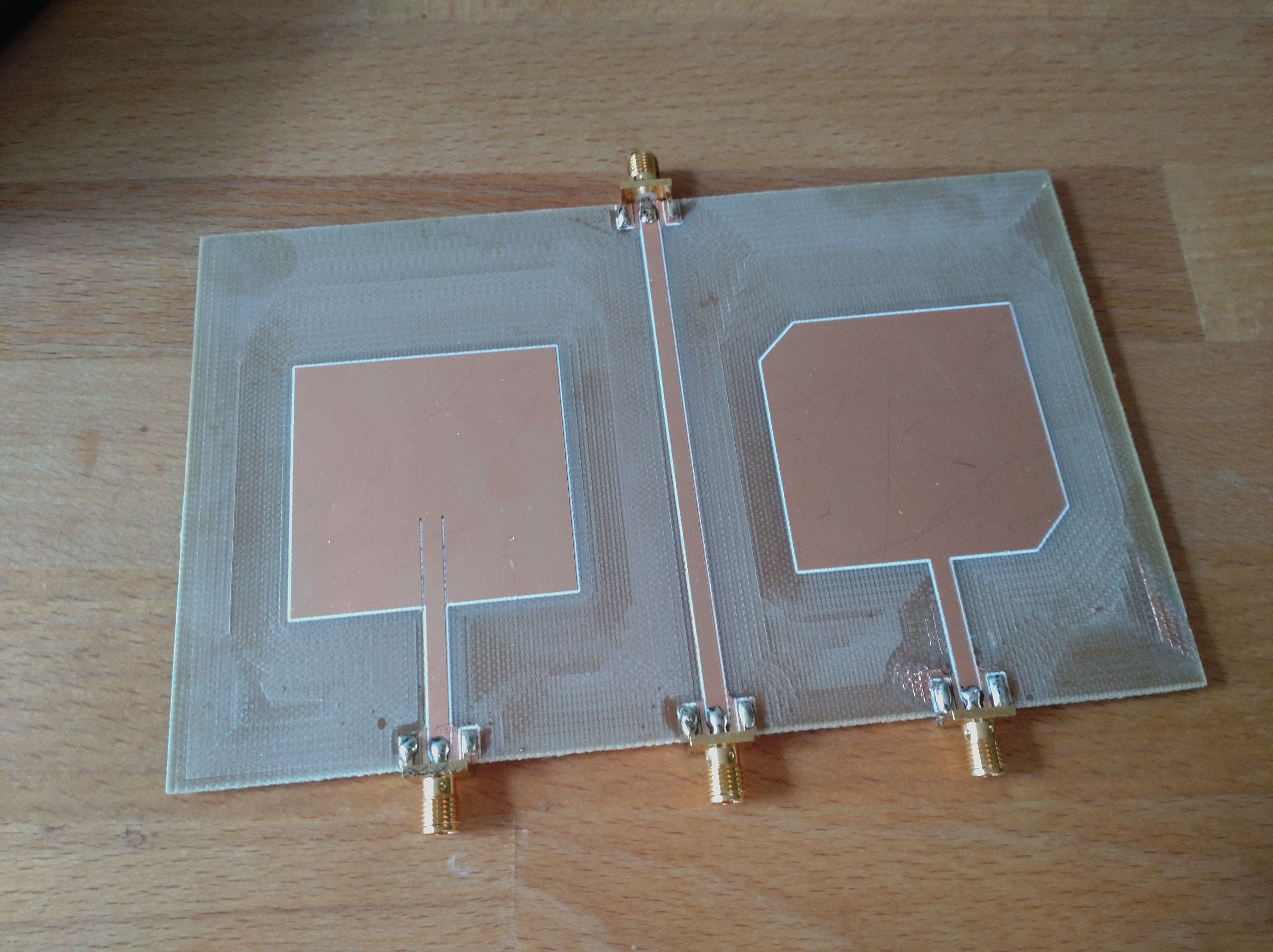
A patch antenna is an antenna of a flat design, which [Pepijn] was going to put directly on a PCB. However, there was added complexity due to GPS being a circularly polarized signal, and that meant doing some research.

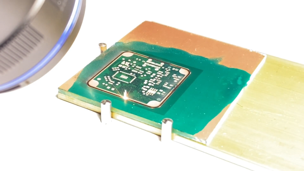
Sadly, nowhere did [Pepijn] encounter a straightforward reference design or examples, but in the end success came from going with a truncated corner patch antenna design and using simulation software to figure out exactly what dimensions were needed. (The openEMS free simulation software didn’t bring success, but the non-free Sonnet with a trial license did the trick.) The resulting PCB may not look particularly complex, but every detail matters in such designs.

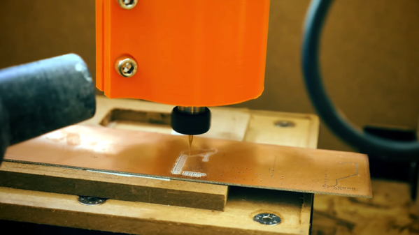
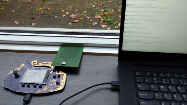
KiCad handled the PCB CAD design but the prototype came from cutting the PCB on a CNC machine instead of having it fabricated and shipped; a much cheaper and faster option for those with access to the right tools. A bit more testing had the prototype looking good, but the real proof came when it successfully received GPS signals and spewed valid NMEA messages. The design files are on GitHub but as [Pepijn] says, the project was about the journey more than anything else.

Laser Blasts Out High-Quality PCBs

With how cheap and how fast custom PCBs have gotten, it almost doesn’t make sense to roll your own anymore, especially when you factor in the messy etching steps and the less than stellar results. That’s not the only way to create a PCB, of course, and if you happen to have access to a 20-Watt fiber laser, you can get some fantastic homemade PCBs that are hard to tell from commercial boards.

Lucikly, [Saulius Lukse] of Kurokesu fame has just such a laser on hand, and with a well-tuned toolchain and a few compromises, he’s able to turn out 0.1-mm pitch PCBs in 30 minutes. The compromises include single-sided boards and no through-holes, but that should still allow for a lot of different useful designs. The process starts with Gerbers going through FlatCAM and then getting imported into EZCAD for the laser. There’s a fair bit of manual tweaking before the laser starts burning away the copper between the traces, which took about 20 passes for 0.035-mm foil on FR4. We have to admit that watching the cutting proceed in the video below is pretty cool.

Once the traces are cut, UV-curable solder resist is applied to the whole board. After curing, the board goes back to the laser for another pass to expose the pads. A final few passes with the laser turned up to 11 cuts the finished board free. We wonder why the laser isn’t used to drill holes; we understand that vias would be hard to connect to the other side, but it seems like through-hole components could be supported. Maybe that’s where [Saulius] is headed with this eventually, since there are traces that terminate in what appears to be via pads.

Whatever the goal, these boards are really slick. We usually see lasers used to remove resist prior to traditional etching, so this is a nice change.

Continue reading “Laser Blasts Out High-Quality PCBs”

CNC Your Own PCB With This Tutorial

It is getting so easy to order a finished printed circuit board that it is tough to justify building your own. But sometimes you really need a board right now. Or maybe you need a lot of fast iterations so you can’t wait for the postal service. [Thomas Sanladerer] shows how he makes PCBs with a CNC machine and has a lot of good advice in the video below.

He starts with Eagle, although, you could use any creation package. He shows what parameters he changes to make sure the traces don’t get eaten away and how to do the CAM job to get the files required to make the boards. If you don’t use Eagle, you’ll need to infer how to do similar changes and get the same kind of output.

We’ve only heard a few people pronounce Gerber (as in Gerber file) with a soft G sound, but we still knew what he meant. We have the same problem with GIF files. However, once you have Gebers, you can join the video’s workflow about 5 minutes in.

At that point, he uses FlatCAM to convert the Gerbers to a single G-code file that integrates the paths and drill files. There were a few tricks he used to make sure all the tracks are picked up. Other tricks include leveling a spoil board by just milling it down and mounting different size bits. He also has ideas on aligning the Z axis.

Continue reading “CNC Your Own PCB With This Tutorial”

Guide: Why Etch A PCB When You Can Mill?

I recall the point I started taking electronics seriously, although excited, a sense of dread followed upon the thought of facing the two main obstacles faced by hobbyists and even professionals: Fabricating you own PCB’s and fiddling with the ever decreasing surface mount footprints. Any resistance to the latter proves futile, expensive, and frankly a bit silly in retrospect. Cheap SMD tools have made it extremely easy to store, place, and solder all things SMD.

Once you’ve restricted all your hobbyist designs/experiments to SMD, how do you go about producing the PCBs needed for prototyping? Personally, I dread the thought of etching my own boards. The process is laborious and involves messy chemicals and specially sensitized PCB’s — none of which interest me. I’ve only ever done it a few times, and have promised myself never to do it again. Professional but cheap PCB manufacturing is more like it board pooling services such as OSH park have made this both easy and affordable — if you can wait for the turnaround.

So what are the alternatives? If you are really serious about swift prototyping from your own Lab, I put forth the case of milling your own PCB’s. Read on as I take you through the typical workflow from design to prototype and convince you to put up with the relatively high start up cost of purchasing a PCB mill.

Continue reading “Guide: Why Etch A PCB When You Can Mill?”