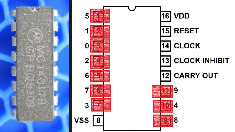
If you’ve ever handled a chip with a really strange or highly inconvenient pinout and suspected that the reason had something to do with the inner workings, you may be interested to see [electronupdate]’s analysis of why the 4017 Decade Counter IC has such a weirdly nonintuitive pinout. It peeks into an IC design dating from the 1970s to see an example of the kind of design issues that can affect physical layout.
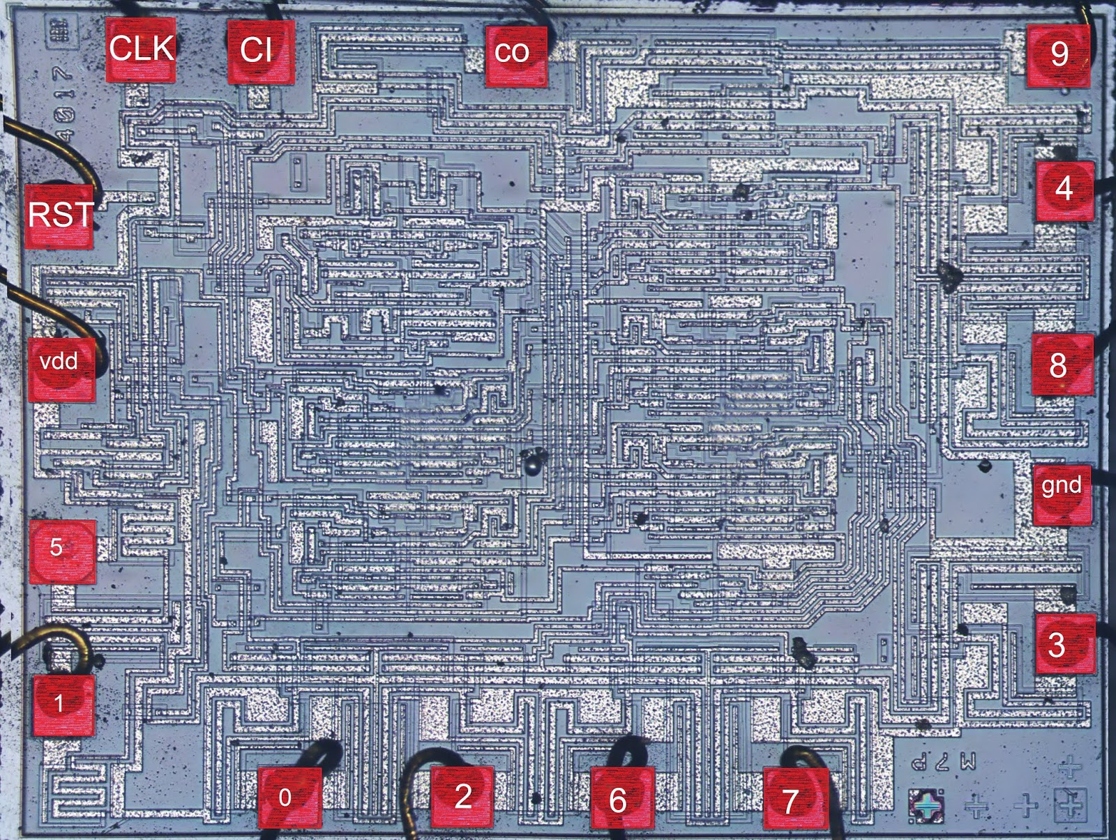
In the case of the 4017, once decapped and the inner workings exposed, things became more clear. Inside the chip are a bunch of flip-flops and NAND gates, laid out in a single layer. Some of the outputs (outputs 5 and 1 for example, physically on pins 1 and 2 respectively) share the same flip-flop.
The original design placed the elements in a way that made the most logical sense for routing and layout, which resulted in nice and tidy inner workings but an apparently illogical pinout. A lot of this is probably feeling familiar to anyone who has designed and routed a single-layer PCB, where being limited to one layer makes it important to get the most connections as directly near one another as possible.
Chip design has of course come a long way since the 70s, but there is forever some level of trade-off to be made between outward tidiness and inner design harmony. The next time you’re looking at a part with an apparently illogical pinout, there’s a fair chance it makes far more sense on the inside.
If any of you are interested in decapping ICs yourselves to see what’s inside, we saw that it’s possible with commonly available chemicals, not just nasty ones.


Yes, of course! IC pad and package pinout is a compromise between die routing constraints and board routing constraints. In this case only die routing constraints were considered. In a complex high speed board design with custom high pin count ICs, you have to factor in board constraints when defining IC pad and package pinouts.
At least you will never have a totally upside-down pin order compared to what you need on your PCB project.
That’s what needlenose pliers are for.
Just mount the part on the other side of the PCB. :P
There are chips supplied in two pinouts so you can mount them top or bottom side with the same connection pattern to adjacent support circuitry. It’s lovely from an evaluation board layout perspective but devilish when you’re the person laying out the production test hardware.
I’ve never seen it, but I remember Zilog’s SIO-0, -1 and -2, with different bonding. They needed 41 pin for the chip when 40-pin was a standard, so they made 3 options which sacrifice different pins.
I have an old Carver Sonic Hologram device that was in my stereo system back in the days when I was into that stuff and long before surround sound. It used some noisy op-amps that I looked into replacing with more modern low-noise chips. I remember the frustration I felt when I discovered that Carver had selected what seemed to be the one quad op-amp chip with a nonstandard pinout. Of course, these days it would be an easy fix to design a breakout board for any desired op-amp, but back then we didn’t have Osh Park.
I still have that device… maybe time to crack it open and see what I can do with it.
I wasn’t sure if I knew about the C-9 back then, so I googled this…
https://www.highfidelityreview.com/carver-c9.html
I guess it wasn’t on my radar back then.
Thanks for this! I started with 555s and simple 40106 oscillators, then I started playing with the 4017 and was completely confused. This makes sense now.
I just want to make beeps and bloops!
Whoops, meant to reply to the general thread, not your comment…
It was great with my Quad ESL-63s and my biamped DIY electrostatic speakers. I found anything that was mixed to give a surround effect in plain stereo went 3D with the C9. Example: Papa Legba on the Talking Heads True Stories Album, and all of the My lIfe in the Bush of Ghosts album by David Byrne and Brian Eno.
Hmmm. Maybe time to dust off some of that gear and fire it up again.
In fairness fabbing a single board or using vero is easy enough.
Osh park is only useful imo for complex or moderate number of boards.
You might even have been able to deadbug
Most of the new parts are available in SMT.
SOIC, TSSOP to DIP on a PCB:
https://www.aliexpress.com/wholesale?catId=0&initiative_id=SB_20200217112146&SearchText=SOIC+to+DIP+PCB
I really don’t mind mixed up pins, what drives me nuts is the wasted pins in a package that’s bigger than it needs to be…like the mcp23018 is a 28 pin dip that only uses 24 pins (2 nc pins on each side). It comes in smd varieties so space inside the package isn’t the issue…the smd versions are even 24 pin. And they changed the addressing enough from the mcp23016/23017 that they are not interchangeable so that’s not it either.
I realize that using a dip package is a space waster to begin with, but they don’t need to make it worse.
Just idly wondering what kind of stuff you’d have to be doing before you have to worry about the sixtieth of a nanosecond propagation difference between the top pins and the middle pins, due to the die hookup being 5mm longer.
>sixtieth of a nanosecond propagation difference
If you are dealing with data window of 100ps where 1/60ns (0.016) would account for 16% of your timing budget, you would care. 10+Gbps isn’t unheard of these days.
I worked on some of the last msi chips. With single layer metal and poly routing, being able to complete all critical connections with short metal was a driver of floorplan placement of transistors and hence pin out. Several reasons..
– Poly and active suck as interconnect layers , the contacts to change layers were also to be minimized. (Yield) Back then most metal connection delays were C dominated. However poly is much higher resistance than metal.
-locality of connection minimizes routing layer resource use , which is one several potential constraints for chip size(cost).
– managing complexity of connection reduction was important when these chips were hand layout. Back in the days of light tables, primitive eda software and coordinate capture devices.
Ah if only we could go 5mm in 17ps!! For modern chips today
With gate delays now way sub ns, on chip propagation delays being hundreds of ps per mm..(rc sucks) it can take multiple high speed clock cycles to cross a 5mm die.
However most chips I have worked on have been a trade off between Pcb driven limitations, escape routing on board, performance, cost, ball pitch. Test concerns, reliability, Esd robustness, …And chip floorplan driven limits, performance, system block diagram, functional locality , block power management and so on…
Many modern catalog MCU chips have big mux trees that allow soft reconfiguration of pinout. Both GP-io and analog pins. Of course some high performance needs preclude that for some pins – serdes, xtal/osc, clocks , power pins etc…
I should include some links to papers on this topic to help but I am on my phone
That’s a lot of great info, learned something new every line of your comment:)
As some one who worked in IC design and layout in the early 1970s, including the 4017, I can attest that hours were spent in reducing the physical size of chips and the only constraints on pinout were the Vcc and Gnd for new designs.
i figure anything that can increase the number of units you can get out of a single wafer would help drive the unit cost down and profits up.
Take a look at some of the very early TTL, like the 7490. Power and ground were in the middle of the package, to reduce the inductance of the bond wires. It keeps you on your toes working with a board that mixes these in with parts with power and ground on the corners.
I ‘member also some early chips had tabs right in the middle there for power and ground, and was wondering if they had some notion of thermal management through bigass central conductors like that.
It was on lower TDP devices. Another variation was a large tab protruding from one end of the device with or without a hold and/or downward tabs forming an upside-down U shape.
Higher TDP devices, particularly audio amps, usually used TO220 style packages.
Expain the Z80 Data pinout: D4 D3 D5 D6 D2 D7 D0 D1
TEMPEST hardening… okay, I’m BSing, unless it gets automatically declassified in another 5 years, then I wasn’t.
Ken Sheriff already explained why:
http://www.righto.com/2014/09/why-z-80s-data-pins-are-scrambled.html
It’s most likely the most convenient places, I am conspiracy theorist, but to think that a hacker would be thwarted by an in-logical pinout is nuts
I was just thinking of the Z80 actually. It is pretty unusual, although I guess it doesn’t matter how you wire the data pins as long as you program your ROM the same way.
Wow! I’ve always been interested why sometimes 2 or 3 outputs of 4017 are in logic 1 after powering the IC up. But I’ve never thought it is because 4017 internally uses the Morse code and it is caused by decoding an invalid Morse number.