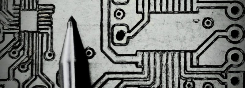
Building a PCB at home can be fraught. If you’re etching, there are chemicals and the nuances of toner transfer. If you’re milling, getting the surface height just right, and not breaking those pointy little v-cutters is always a challenge. [Robin] has tips for both of these cases, and solves a lot of the common hassles by using a milling machine.
Whether he’s scraping away etch resist or entire copper isolation lines, [Robin] uses a non-spinning scratching tool instead of a v-bit: they’re more robust and cut every bit as well. He’s got tips for using FlatCam and KiCAD to make scratched-out traces. His registration system allows him to get double-sided boards with a minimum of hassle. And as a bonus, he’s doing some experimentation with embedding SMT parts inside the boards as well. Be sure that you check out his whole guide, or just watch the video embedded below.
We’re pretty sure you’ll pick up a trick or two, and maybe you’ll be convinced to bite the bullet and invest in a nice mill. If you’d like a more traditional take on PCB milling, try out our own [Adil Malik]’s guide.


The title should have been “MAKING PCBS THE HARD WAY” . Why anyone in the world would even bother wasting their time on doing it this way anymore amazes me. You can get qty. 5, 4″ x 4″ pcb with mask and silkscreen for like $6.00 all day long now. Just makes no sense.
Here, turnaround for china orders is between 1.5 and 3 weeks. So for quick prototyping – why not.
Local pcb factory gives 3-4 day turnaround for quck orders, but they are more than 6$.
If I’m working on something I don’t want to wait that long for the next iteration or parts to arrive (though I still have to far too often). Homefab might be more expensive in both materials and your own time investment and still be really worth it as do you don’t have to wait for shipping/customs so can actually get your project done much faster.
If you only do really really simple PCB were no dimension or layout feature is critical you will probably get something that works first time. But anything with complex layout – highspeed, precision pads for tiny ball grids/small pcb layer connectors its never going to be perfect on the first run, it might not even work at all, so being able to get it perfected with the undoubtably larger features than the profab can provide so if it works on your homemade it will work when outsourced. And if its a one off bespoke board you only need one of them this is perfection (and should you then recreate the project the design is already valid and should be trivial to outsource if you want to)!!
And what I’ve seen so far of this method looks like it might well become the method I adopt for my next pcb have to do some more looking at its limitation etc but it looks damn neat.
When shipping for those $6 PCBs still costs $35 minimum, not even thinking about customs procedures and fees, this is definitely still the easy way.
No, the first cheap Chinese PCB manufacturer I tried wants $14.66 for five 10x10cm boards incl. shipping to the US. The shipping is less when the boards are smaller.
In my country I do not (yet) have to deal with customs and VAT when importing something that cheap.
For shipping to Turkey, both Chinese PCB manufacturers I’ve looked at only have DHL available for $35 on top of the PCB manufacturing cost (admittedly, fairly cheap). Plus, I also have to deal with both customs and VAT for anything above $0 – and I’ve had PCB deliveries refused before because I was ordering “commercial quantities”. OSHpark is a plausible option with free shipping worldwide – but I haven’t had a chance to try them out yet (do want to, though).
Consider it “just in time” and prototyping manufacturing.
When testing things or dealing with time limited things, it’s best to keep it local.
Some people like a challenge, and the resulting satisfaction of completing it.
Sending money to China and waiting for a poorly wrapped package to arrive weeks later isn’t much of a challenge.
Here in Brazil-land, you can pay $6×5 = R$30. And add R$200 (for the shipping/taxes too. Something like R$230 ($46) after 1 to 4 months of waiting for a bunch of small dummy and naked boards is not good at all.
Your comment basically amounts to, “the easy way to make PCBs is to not make PCBs.”
Don’t forget those 4″ x 4″ pcbs are double sided with plated through holes, with 6 mil traces on 6 mil spaces design rules.
I think for prototyping -and learning- it is hard to beat home made PCBs. With simple boards taking well under and hour, it’s close to breadboarding, but allows using SMD chips. Once you are happy with the prototype, getting the board made professionally is definitely the right call. And if it was just for learning, the trash drawer is fine given the effort and cost :).
@Mike – Why bother soldering things together yourself when you can get just about any gadget already assembled delivered straight to your front door for only a few dollars these days?
\Sarcasm
I was kind of disappointed to see that so many are so rabidly anti-home PCB production. Besides the practical consideration that even a small turn around becomes a lot of time spent waiting after a few iterations doing it oneself is kind of part of the point right?
Yah, I know. Carl Sagan was not wrong when he said “If you wish to make an apple pie from scratch, you must first invent the universe.”. We all HAVE to draw a line somewhere. But why be so discouraging when someone draws their line at a lower level than you do?
Now I think I do get it. @Mike and others are jealous of those who have more abilities than themselves! Hey, I get it, me too. But that’s why I keep learning. No need to tear down others efforts.
I totally agree. Just nutso to mill it. You can laser print on transparency film and photo etch a board with less BS and there are a lot of chemistry available for etching.
I for one don’t want to mess around with the hassle and danger of chemical etchings. I am much more comfortable putting a pcb in my mill than in a vat of acid.
Got no problems with folks wanting to etch – but mills do have a few advantages – its a machine that can do other things as well being the big one.
You also have the storage/desposal/refreshing of your etchant which is probably a bottle as big as the smaller pcb mills. Not to mention you need a tank and for really good results on the fine traces a spray/agiitation system so the whole thing etches evenly, which can be even more space than a mill again.
Oh and your mill can also do the through holes itself something you have to do yourself with etching.
Both are good methods, so its stupid to call using a mill ‘nutso’ its another simple and effective method to make a board. And once you get the method mastered its less manual effort than any home etching system I’ve seen (I have been known to home etch myself, but haven’t yet made my mill cnc despite how useful that could be (it would also need some precision upgrades for this level of work I’d think)).
Some times you need the PCB today, some times you need it now. So is good to know new technics because it can save your ass.
True, but when finishing my senior capstone project last year there were times I needed a PCB/breakout overnight. My college had a milling machine, it made “good enough” PCBs the same day.
It starts making a whole lot of sense if you need to tweak something, and you need it now. For production, nothing beats professional manufacturers, but for prototyping, homebrew PCBs rock!
I believe the word is “fraught,” not “frought.”
Yes, I’m not the only one driven crazy by that word! And is not an adjective, so perhaps the experience was “fraught with peril”.
Fixed, thanks.
I woke up this morning to no T-Mobile home internet. My router is up on the roof, and after disassembly it seems to connect with pogo pins to some frame with copper strips for LTE & wifi. I de-soldered a bluetooth serial thing I’ve been saving just for this & stole the ANT connector. I also have a LTE repeater thing with a pad ANT. I cut a no copper section out of a previously etched board and used this copper tape I ordered from wish a while ago. put it together & clamped with a HF plastic C clamp. I woke up 6:30 am with no netz, and had it up by 8am. I may eventually 3d print the frame with a connector on it ( a couple actually), but for fast prototyping the copper tape is the really fast way. No way was I waiting for acid.
I really want to explore copper and aluminium tape more. Even if just wrapping power and ground bars along the top and bottom sides. I don’t have access to a laser this month, but I wonder if the covering of copper tape would burn off with a laser? That would make easy accurate etching, and maybe you could tape it to something that would allow laser cutting drill holes once it was etched. Maybe it just melts and puddles though, not sure.
I use a laser engraver the same way to remove the spray paint coat from the copper before the acid. Quick and simple.
What spray paint do you use? I’ve been trying the same thing but it leaves a slight residue which hinders the etching.
I had problems with residue when I tried it as well. The closest I came to a solution was to do a second pass to clean up most of it. Also the green solder mask on professionally made boards burns away beautifully in the laser cutter. Super glue seemed to work ok too.
I use An automitive type touch up spray in mat black. After the laser marking, I use a cotton ball with alcohol to clean the residue. If you don’t apply much pressure it will not harm the spray paint. It’s very important to let the paint dry thoroughly.
I use the same method on stainless steel to electro etch name plates and figures. I paint a
On both sides of the plate and leave a small area to clamp a small bolt and but to connect the wire. I use salty water and a small DC power supply
I’ve never ever broken a V-bit. End mills and 0.8 mm drills may break, but I can’t really see how you could break a V-bit.
It’s very easy.
All it takes is a little mistake in programming a CNC machine. Just have a look at “CNC Crash” on youtube and you’ll find plenty of broken mills and worse.
Crashes of CNC machines are so common (and expensive) that some manufacturers put in special break plates to save the spindle motors and bearings in such events.
lol.. it is very easy to screw up a z coordinate or proper homing/zeroing and drive that v-bit right thru the board mdf and all… sometimes without the spindle running… my cnc will snap a 1/8 bit clean off…. the the tip is easy too…
I broke at least three bits by hitting the holding screw. On few occasions a piece of stock was lifted because tabs were too thin and too weak, and jammed the mill against rest of the stock. That\s why I keep an eye on the machine during work…
I’ve had the tip of 0.1mm 10deg V-bit break off many times. Not sure why, it seems to be quite random. Maybe some scarf gets it wrong place of something. 0.3mm 30deg is more robust but makes quite wide grooves.
A diamond tipped tool as used for engraving glass works a treat. I have done this a few times on an engraving machine and have found that spinning the tool at about 1000 rpm makes for a very clean finish. Roland engraver suppliers have them. Part number ZDC-A4000
I’m also interested in this, partly for small simple things, and mostly for the quick turnaround time for prototyping. Take for example the design and verification of PCB antenna’s. With this setup you can have a new revision in several minutes to half an hour, depending on how good the software works.
I’m already a bit familiar with bCNC, and I knew of the existence of Flatcam, and this post gave me some motivation to experiment with flatcam. I had some installation difficulties, but in an hour or so I managed to get it to the point that I had a version of Flatcam that has generated G-code and have loaded it in bCNC.
Long straight lines are single G01 vectors, but arcs and circles are not recogniezed as such. A single round pad can easily be 60 G01 vectors. Not a huge deal, but it does increase file size.
The version I now have running is 8.5 according to the about box, but it runs in Python3 (Yippee).
I did read somewhre that the Python3 port was in 2018, so I do not know what’s going on there.
I am trying to make some notes as I go along. Here is my history of installing dependencies both with apt and with pip3. The last try with pip3 and the “requirements.txt” got me to a point I could run Flatcam.
2001 apt search flatcam
2002 pip3 search flatcam
2003 pip3 install flatcam
2004 cd projects/python3/
2005 git clone https://bitbucket.org/jpcgt/flatcam
2006 cd flatcam
2007 python3 flatcam
2008 python flatcam
2009 apt search PyQt4
2010 sudo apt install python3-pyqt4
2011 python3 flatcam
2012 apt search simplejson
2013 sudo apt install python3-simplejson
2014 python3 flatcam
2015 python flatcam –version
2016 python3 flatcam
2017 sudo apt install python3-rtree
2018 python3 flatcam
2019 sudo apt install python3-svg.path
2020 python3 flatcam
2021 cd sandbox/
2022 python3 diagnose.py
2023 cd ..
2024 ./setup_ubuntu.sh
2025 python3 flatcam
2026 python3 setup.py
2027 Python ./FlatCAM.py
2028 python3 ./FlatCAM.py
2029 ls
2030 pip3 install -r requirements.txt
2031 python3 flatcam
2032 history
The vast majority of CAM software has abandoned G02 and G03 for a ton of G01 commands. I think this is in part because it’s more flexible (elliptical and b-spline are supported), in part because there are g-code interpreters out there that don’t acknowledge g02/03 anymore, and in part because on some machines, g02/03 arcs over a large radius were inaccurate.
I like bCNC as a mach3 replacement.. for pcb i started using https://github.com/martin2250/OpenCNCPilot it was just dead simple for pcb making… autolevel and gcode (i mostly run win)
That looks like a great option, thanks for the link!
Now FlatCAM project Is in progress with new features
https://www.mischianti.org/category/tutorial/flatcam-complete-tutorial/
I order (2-layer) PCB’s from JLC-PCB at $2-5 (bundle a couple of projects to make $12) and receive them within a week using DHL for $23 extra (currently a week and a half). I sometimes choose some of the less expensive shipping methods if it can wait (adds a couple of weeks). After JLC-PCB has accepted the order, I order the corresponding components from Mouser (because they pay incoterms and DigiKey does not) and receive them a day before the PCB’s arrive at $0 for shipping (when ordering for more than $50 which I always plan for). This scheme has served very my well for many hobby projects over the last few years. I would never consider fabricating them myself nowadays, but I understand that the conditions change from country to country, which is also often the killer for us here in the EU in other regards.
I had an LPKF Promat s62 ‘professional’ rapid prototyping PCB mill at one point.
An expensive mistake in my humble opinion , given the price of finished masked PCB’s these days.
It comes with a million and one little gotchas in it’s own rights , even on the pro machines. Forget about BGA or anything fine pitched.
For example in TSSOP28 was right at the very limit even with your tongue at the right angle and the gods smiling down , slightest variation in copper thickness and it was a wash out and bear in mind this was with a piece of very expensive kit engineered to do the job.
Helder Ferreira I think is on to a better DIY approach IMHO , laser ablation of an enchant mask.
LPKF actually do a direct copper ablation system (protolaser) but that really is megabucks.
I use a blu-ray laser for exposing photoresist and solder mask. I am getting very good results with presensitized PCBs.
https://hackaday.io/project/26216-pcb-exposer
Your PCB design better not have many vias. Plugging those non-through-plated holes with bits of wire that have to be soldered on both sides could add up.
Step one: have a cnc mill
Well, failed that one pretty quickly
Yep!
B^)
Hehehe.. resolved with new target
https://www.mischianti.org/category/tutorial/cyclone-pcb-factory-how-to-build-it/
But pcb milling become a drug
I’ve spent enormous amounts of time and money trying almost every form of home PCB manufacture. Photoresist, thermal transfer, home-built PCB mill , etc… I’ve learned the hard way that the best way to make PCBs is… DON’T.
Seriously, unless you have an emergency need, use one of the dirt-cheap online services. You’ll get a better PCB, and you WILL spend less. You’ll get better results. You’ll get silkscreen, solder mask, plated vias…. You WON’T get evil splinters. You won’t be exposed to, or need to store toxic reagents. You won’t be limited to tiny sizes….
The “solder masks and silk screens” thing is why I haven’t been doing much of my own PCB work even though I own a router that’s good for it. It feels good to make a board yourself, but the commercial boards are much nicer to populate, and hold up better to handling.
Solder mask isn’t a big problem at home https://www.mischianti.org/2019/03/14/design-and-mill-pcb-easy-and-cheap-part-5/
But commercial board is surely better.
Where are all these cheap PCB manufacturers ? I have contacted a number to get a 218×120 prototype made and all wont make less that 5 boards. The board cost + shipping comes to $174 US including shipping then convert the currency into Aus dollars and you have some very expensive PCB’s. I see adverts on the net claiming PCB’s for $1, and $10 well I have yet to come across them.
“Everyone” seems to use JLCPCB, even though the company does not guarantee they won’t make mistakes. In that case, resist the temptation to get mad, or even call them to complain, just be grateful for their low, low prices, and resubmit the job.
The main external link in the article went stale (“404”).
Here is an Internet Archive “Wayback Machine” snapshot from 2020:
https://web.archive.org/web/20200616063418/http://debreuil.com/blog/pcbs/scratch-milling-pcbs-at-home/
Maybe the Hackaday editors can insert it into the article? (like Wikepedia volunteer maintainers do)