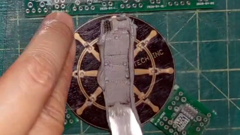
Imagine having a surface mount kit that you’d like to stencil with solder paste and reflow solder, but which doesn’t come with a solder stencil. That was what faced [Honghong Lu], and she rose to the challenge by taking a piece of PET sheet cut from discarded packaging and hand-cutting her own stencil. It’s not a huge kit, the Technologia Incognita 2020 kit, but her home-made stencil still does an effective job.
So how does one create a solder stencil from household waste? In the video we’ve put below the break, she starts with her packaging, and cuts from it a square of PET sheet. It’s 0.24mm thick, which is ideal for the purpose. She then lays it over the PCB and marks all the pads with a marker pen, before cutting or drilling the holes for the pads. The underside is then sanded to remove protruding swarf, and the stencil can then be used in the normal way. She proves it by stenciling the solder paste, hand placing the parts, and reflowing the solder on a hotplate.
It’s clear that this is best suited to smaller numbers of larger components, and we’ll never use it to replace a laser-cut stencil for a thousand tiny 0201 discretes. But that’s not the point here, it’s an interesting technique for those less complex boards, and it’s something that can be tried by anyone who is curious to give stenciling and reflowing a go and who doesn’t have a project with a ready-cut stencil. And for that we like it.
Making your own stencils doesn’t have to include this rather basic method. They can be etched, or even 3D printed.


LOVE the low budget approach!
if you happen to have a cutting plotter and transparent printable sheets you can use those aswell. even after running 1000 pcbs through one sheet they still work fine for me. (there was an article on here a few years back about this technique.
Even for small series, I 3D print mine. It´s fast to produce, fast to print, lasts enough for dozens of boards if you´re careful, and costs pretty much nothing. I would not go the hassle of cutting any by hand, even for just few 1206s
fantastic idea, please do tell, sla? what thickness is the final stencil? and layer height are you using?
There are various tutorials of 3D printed solder stencils on YT.
Awesome, thanks
You don’t have to go all that far to find some great examples:
https://hackaday.com/2016/02/08/solder-stencils-with-a-3d-printer/
https://hackaday.com/2020/03/27/can-solder-paste-stencils-be-3d-printed-they-can/
Can you do 0603 or smaller and 0,5mm fine pitch that way?
neat. i sort of imagined someone sitting there cutting the pads out with an xacto knife when i first saw the title.
the drill works surprisingly well. i’d be interested in seeing some cheap plastic CNC’d with a fine end mill to accomplish this.
I’d figure that round holes would work quite well for some components, because they have the lowest circumference (= drag) to area ratio. and the paste will flow anyway.
But re-tracing the PCB with a marker would be a bore. Why not simply print the stencil on paper and use that as a template (on either top or bottom of the PET), or, if available, print it on overhead sheet (if those things still exist)
Print out on overhead film, drill out the holes. That’s pretty darn good.
I forgot to add:
Round holes may work well for resistors even down to 0201 or maybe even smaller.
But I do think you may get into trouble for IC’s with many leads and fine pitch such as QFN. With round holes you may not have enough solder before the holes start overlapping.
in that case maybe two overlapping small holes would work better, or use a small drill and drag the sheet a little bit with the drill in the hole for an oblong hole
I been using gerber to graphtec program for years using a mylar stencil cutter.
It just works for any board of all sizes.
https://github.com/pmonta/gerber2graphtec
https://hackaday.com/2012/12/27/diy-smd-stencils-made-with-a-craft-cutter/
I wonder if mylar would be suitable.
You can get 7mil-thick sheets that cut well with a CO2 laser, for the purposes of paint stencils. But could they work with solder paste too? It doesn’t seem far-fetched.
I do not know about the behavior of mil-spec’d mylar sheets. But normal 100µm mylar bought as overhead transparency film worked quite OK. Probably I could have optimized the cutting parameters a little more to get less burs from partially molten material. Kapton would have been better, but I did not have it – and what I had least was time (to wait for an ordered commercially made stencil). So I went to my local hackerspace with it’s CO2 laser cutter and took a spare FR4 PCB to scrape off most of the cutting burrs.
The 0,5mm fine pitch ICs took some manual rework after reflow, but it was much faster that way than hand soldering.
I’ve always made masks for surface mount parts with scraps of plastic film, usually the clear windows from cardboard packaging. I’ve never been one to throw things away. I also use thicker sheet plastic masks to locate the parts on the board prior to soldering, smd and tremors don’t usually mix terribly well.
We used it a lot just because it was handy and fast in 2005~2008 before the laser cut stencil are cheap in China. Mostly we use 0.1mm~0.15mm thickness ones because we had them for printing the design for pcb to review and also thicker one sfor test rig in mfc. It is good for 0603 component and sth bigger than it.
I just use a sheet of regular paper and a laser cutter for those times I only make 1-5 boards.
It can hold up for a handful of boards. And paper can be ordered in a lot of different thicknesses and is trivial to get, and also dirt cheap. (typical 80 gram/m^2 paper is a bit “thick”, but for 0603 packages and similar sized devices it works fine.)
My weapon of choice for prototype stencils is Kapton film sheets on an Epilog Legend 75 watt laser. A mix of rastering through the film and using a vector line for edge cleaning can make for some very small and precise apertures to make garage mounting of QFNs and BGAs very reliable.