
Were it not for the thin sheath of water and carbon-based life covering it, our home planet would perhaps be best known as the “Silicon World.” More than a quarter of the mass of the Earth’s crust is silicon, and together with oxygen, the silicate minerals form about 90% of the thin shell of rock that floats on the Earth’s mantle. Silicon is the bedrock of our world, and it’s literally as common as dirt.
But just because we have a lot of it doesn’t mean we have much of it in its pure form. And it’s only in its purest form that silicon becomes the stuff that brought our world into the Information Age. Elemental silicon is very rare, though, and so getting appreciable amounts of the metalloid that’s pure enough to be useful requires some pretty energy- and resource-intensive mining and refining operations. These operations use some pretty interesting chemistry and a few neat tricks, and when scaled up to industrial levels, they pose unique challenges that require some pretty clever engineering to deal with.
Hard as Rock
The raw material for most silicon production is the mineral quartzite. Quartzite comes from ancient deposits of quartz sands that formed sedimentary deposits. Over time and with heat and pressure, these quartz sandstones were transformed into the metamorphic rock quartzite, which is at least 80% quartz by volume.
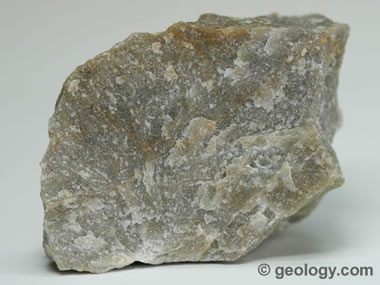
Quartzite is an incredibly tough rock, and where it pokes above the surface, it forms ridges that strongly resist weathering. Significant formations of quartzite are scattered all around the world, but there are relatively few places where it makes financial sense to quarry the rock for silicon production, since the formations need to be easily accessible and relatively close to the other raw materials and energy supply needed.
Raw quartzite is mostly silicon dioxide (SiO2), and the refining process begins with a reduction reaction to get rid of the oxygen. Crushed quartzite is mixed with carbon in the form of coke (coal that has been heated in the absence of oxygen). Woodchips are added to the charge as well; they serve both as a carbon source and a physical bulking agent that allows gasses and heat to circulate better in the furnace.
The arc furnaces for silicon smelting are massive installations with huge carbon electrodes. The electrodes are consumed during smelting, so new electrodes are screwed onto the tops of the current electrodes to make sure the process isn’t interrupted. The arc furnace requires massive amounts of electricity to maintain the 2,000°C temperature needed, so silicon refineries are often located where electricity is cheap and plentiful.
The reduction reactions inside the melt zone are actually pretty complicated, but can be summed up with two main reactions:

In both reactions, the oxygen in the silicon dioxide combines with carbon to form the main waste product, carbon monoxide. A side reaction that occurs in a part of the melt zone inside the furnace produces silicon carbide (SiC), which is an unwanted byproduct (at least when the goal is to purify silicon; silicon carbide itself is a useful industrial abrasive). By making sure that silicon dioxide is far in excess in the furnace, the second reaction where the SiC acts as a carbon source for the reduction of silicon dioxide is favored, and silicon with up to 99% purity can be tapped off the bottom of the furnace.
The silicon produced by this process is referred to as metallurgical silicon. For almost all industrial uses, this highly purified silicon is good enough. About 70% of metallurgical silicon goes to the manufacture of metal alloys such as ferrosilicon as well as aluminum-silicon, an alloy that contracts minimally upon cooling and is therefore used to cast aluminum engine blocks and similar items.
More Nines
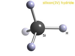
As useful as metallurgical silicon is, even at 99% pure it’s not even close to the purity needed for semiconductor and photovoltaic applications. The next steps in purification take the silicon to the purity level that’s needed for semiconductor manufacture. Purification starts by mixing powdered metallurgical silicon with hot, gaseous hydrochloric acid. This reaction produces silanes, which are compounds with a central silicon atom surrounded by four attachments, in this case three chlorine atoms and one hydrogen. This trichlorosilane is a gas at the temperature inside the reaction chamber, which makes it easier to handle and purify by fractional distillation.
When the trichlorosilane gas has been sufficiently purified, polycrystalline silicon production can begin. The Siemens process is the main method here, and is a form of chemical vapor deposition. A large bell-shaped reaction chamber contains several thin threads of highly purified silicon, which are heated to 1,150°C by passing an electric current through them. A mixture of gaseous trichlorosilane and hydrogen flows into the chamber; the gas decomposes on the hot electrode leaving behind the silicon, which accretes into rods that are about 15 cm in diameter. Polycrystalline silicon made by the Siemens process can have a purity of 99.99999% (“seven nines”, or 7N) or more. 7N to 10N polysilicon is mostly used for photovoltaic cells, although some polysilicon in this purity range also makes it into MOSFET and CMOS semiconductors.
While the Siemens process is the polysilicon workhorse, it has its disadvantages. The main problem is that it’s an energy hog — keeping the growing polycrystalline rods hot enough to decompose the feedstock requires a lot of electricity. To work around this problem, a fluidized bed reactor (FBR) process is sometimes used. An FBR reactor is shaped like a tall tower, the walls of which are lined with a quartz tube. Silane gas, either the familiar trichlorosilane or monosilane, which is just a silicon atom surrounded by four hydrogens, is injected into the chamber. Powdered silicon is dropped into the reaction chamber from the top, while heated hydrogen gas is injected into the bottom of the chamber through a series of nozzles. The gas flow keeps the hot silicon powder fluidized, allowing it to mix with the silane gas and decompose it. As in the Siemens process, the silicon accretes onto the seed particles, which eventually get too large for the fluidized bed to support. The polycrystalline silicon beads drop to the bottom of the chamber, where they can be collected.
Aside from power savings — up to 90% less when using monosilane as a feedstock — the FBR method’s main advantage is that it’s a continuous process, since the finished beads can just be pumped out of the chamber. The Siemens process is more of a batch process, since the reactor chamber has to be opened to remove the polysilicon rods when they’re finished. That said, FBR polysilicon hasn’t really taken off, in part because managing the fluid dynamics inside the reaction chamber can be difficult. But the main reason is that the Siemens process is just so easy, and as long as factories can be located near a source of cheap electricity, it’s just easier to use the brute-force method.
One Crystal Only, Please
Using either of these methods, polycrystalline silicon can be brought to extremely high purity, up to 11N. But purity isn’t the only metric for silicon; sometimes, the nature of the crystalline structure on the end product is just as important as purity. The next step in silicon production is the creation of monocrystalline silicon, where the entire silicon ingot is a single crystal.
Growing a single crystal of ultra-pure silicon to a size that’s industrially useful is no mean feat, and relies on some tricks discovered in 1916 by Polish chemist Jan Czochralski. We’ve covered the Czochralski method in depth before, but briefly, polycrystalline silicon is melted in a quartz crucible in an inert atmosphere. A puller rod bearing a single ultra-pure silicon crystal that is very precisely oriented is lowered into the molten silicon. The seed crystal causes silicon to condense, continuing the crystal structure as the puller rod is slowly withdrawn from the furnace while rotating. Single-crystal ingots up to 450 mm in diameter are possible with the Czochralski method.
Another method to produce monocrystalline silicon is the float zone method, which uses a polycrystalline silicon rod as the starting material. Inside a reaction chamber with an inert gas atmosphere, a radio frequency signal is passed through a coil that surrounds the rod. The RF signal heats the polysilicon, creating a confined melt zone. Single crystals of ultra-pure silicon are added to the melt zone, which causes the molten silicon to crystallize around it. The RF coil is slowly moved up the rod, moving the zone of heating until the entire rod is a single crystal of silicon. Float-zone monocrystalline silicon has the advantage of never being in contact with the quartz walls of the Czochralski method crucible, and so will have less contamination from oxygen and other impurities.


love these articles! It is fascinating to learn how the things we take for granted are incredibly complex all the way down the chain
And also why it’s so difficult to “close the loop” with renewable energy: the processes to manufacture e.g. solar panels requires tons of coal and energy at very low prices. Imagine the cost of a solar panel if you had to make the carbon (out of what?) to make the silicon. Also, why most solar panels are made in China.
“MYTH #1: Solar panels require more energy to manufacture than they produce in their lifetime. FACT: A study by the National Renewable Energy Laboratory conclusively demonstrates that the manufacturing energy cost versus the energy production payback for solar modules is generally less than 4 years”
https://solarcraft.com/solar-energy-myths-facts/
Did you read the “study” ? This is a 2 page paper conveniently crossing numbers from external studies and they systematically take the best case / optimistic scenarios…
Just having a quick look, quoting the 2 page paper : “To calculate payback, Dutch researcher Erik Alsema […] “best estimates”* of energy used to make near-future, frameless PV were 600 kWh/m2 for single-crystal-silicon modules and 420 kWh/m2…”
The very Alsema study (google the title it is public) states : “Published estimates for the energy requirement of present-day crystalline silicon modules vary considerably: between 2400 and 7600 MJ/m² for multi-crystalline (mc-Si) technology and between 5300 and 16500 MJ/m²
so it would go from 2400 to 7600 (5300 to 16500) so from 3 to 9.5 (9.3) years (just back of the envelope proportionality) which is very close to half the service lifetime of a panel….
Plus that doesn’t take into account the energy source used to produce the electricity (as stated before most probably coal and not something “clean”)…
MYTH1 : stating MYTH and FACT without checking the data ain’t good enough for these pages…
*read : ‘we present it as the best quality estimate but actually it is the best case scenario’
…which suggests an EROEI of slightly over 2. The problem there is, even if you have a positive energy return, the society cannot function with energy sources that have an EROEI lower than about 3 because a third of all the effort expended by the society would be spent on making energy. That would be dire energy poverty with serious impacts on living standards, resulting in widespread economic poverty. Practically speaking, if your energy sources drop below 6 in EROEI, you will get riots because everything starts costing too much money for the bottom half of the society.
Not the question, but close.
If you had to manufacture solar panels using solar energy and the other variable and intermittent non dispatchable sources of electricity as your only supply, and make all the chemicals synthetically in a closed loop with proper waste management, the process using presently known technologies would be so complicated and inefficient that your EROEI would become less than 1.
As solar panels and the related materials are by and large made with cheap coal and cheap fossil fuels for energy, and we’re omitting their recycling, and in some cases/places even omitting the waste processing to save cost/energy (dumping spent chemicals in the environment), the EROEI of solar energy is indeed greater than 1 – but this is not a sustainable solution.
This ones a more recent report:
https://www.ise.fraunhofer.de/content/dam/ise/de/documents/publications/studies/Photovoltaics-Report.pdf (page 31 – 36)
All the cites in the NREL study are from 1999, so I don’t get why we are discussing those numbers here.
I don’t get it either, because it’s not even the argument. The EPBT is still assuming production by cheap fossil fuels, since alternative and sustainable processes are simply not used for the cost of it.
If you couldn’t refine silicon by cheap carbon from coal, how much more energy would you need to do it? What raw materials would you use?
While the clip showed Si being produced with renewable hydroelectricity, there is no reason why wind and solar energy will not contribute increasingly as dinosaur burning power plants go extinct. A number of them have done that already here in Australia, as fossil fuelled generation is so expensive that they go broke, one after the other.
It certainly does not take long for a PV array to generate the energy of its creation. My brother’s 20 kW array has generated 15 MWh in 13 months. The clip states one tonne of Si requires 10 to 12 MWh. If the 50 panels of the 20 kW array contain 20 kg of Si each, that’s exactly one tonne, and was energy recovered in ten months, with the remaining 24 years of service life being cherry on top. (The Al frame, if there is one, is 95+% recyclable, so maybe adds less than another month.) Mind you, we have so much insolation here, and so much desert to fill with PV arrays, that there are plans to power chunks of Asia from Darwin, beginning with Singapore. The long HVDC extension cord is no big deal, as China has already done one over land. So, yes, coal is a dead man walking.
With desalination, we can plant millions of hectares of forest for the woodchips and carbon needed for Si production. That would take the carbon from the air instead of dead dinosaurs, making Si production entirely carbon neutral. Given water, there’s no shortage of land here – hundreds of millions of hectares which could be put under forest, even though not good enough for farming, and only used for holding up the sky.
In reality, the only low cost energy is wind, solar, and hydroelectric, now. (And nuclear is the most expensive.)
The PV silicon cells are quite thin, less than 1 mm, often only 300µm. Your 400W panels can have around 2m². 2m² * 0,3mm are 0,6 liter or about 1,4kg of siliconm not 20kg.
Martin, then what are the denialists on about? Rather than recoupment of embodied energy being a cause of concern, solar PV puts everything else to shame. With only 70 kg of Si in the 20 kW array, Si refinement energy is recouped in 42 hours of full intensity operation. Subsequent ingot growing, diamond saw slicing, and doping adds a few percent. Even when we add in the highly recyclable Al frame, the array recoups all embodied energy in weeks.
Is it just because expensive dirty coal never recoups any of the enormous embodied energy of its generation monstrosities, but merely adds further energy deficit during operation, that this Furphy is cranked out?
The sooner pumped hydro, hot rocks, and batteries replace the filthy dinosaur burners, the less our children will be roasted, toasted, and crisped.
its not just the payback its the fact that the array will produce power many hours a day, almost everyday for 30 years. its all about the hours. hence kWh.
“The long HVDC extension cord is no big deal, as China has already done one over land.”
Be careful what you assume abut Sun Cable, there’s the Sunda Trench (>7,000 km maximum depth) and the Timor Trough (>2,500 m maximum depth IIRC) between Australian mainland and Singapore. An overland cable is much easier to deploy and maintain that a subsea cable in some of the deepest parts of the world oceans. I wouldn’t assume it is a done deal just yet.
Many LCA studies have now shown that the embedded energy in typical PV polycrystaline silicon PV panels is paid off in a short time that represents a small percentage of their lifespan. Also panels are rated at a certain power output for their designated lifetime, but they continue producing power at less than the warrentied output rating for years to come. These days the horror shows of delaminating panels and so on is much rarer occurrence. And as RE increases it’ penetration into the mix the electrical energy footprint drops. WA for instance is at ~30% RE and could easily go to 90%-100% within less than ten years if the political and social will was demanding and driving the transition.
People mentioned coal, there’s two side to the coal use, one is as a reductant (and energy source via combustion) for the oxygen in SiO₂ / SiO which then produces CO₂ which I vented into the atmpospere, smelters tend to me colocated with cheap power, which historically has been coal or as mentioned in the video, hydro. There’s a three pot smelter in Western Australia (Simcoa) and they transport the Quartzite rock from mid-west WA down to SW WA in long trains to smelt it there because there is/was a ready supply of coal and native forest timber (which they shouldn’t be taking because it has high conservation value for a few species of endangered black cockatoos).
The other coal usage is in coal fired power plants that often power the arc furnace with electrical power. Historically coal was the cheapest form of power in many places and so those emissions are the ones typically counted for the silicone used to prepare polysilicon. They also burn gas at Simcoa to keep parts of the equipment in a hot-ready state. So coal, native forest timber shredded into would chips and fossil gas. Plus the venting CO₂ from the smelter. Plus the energy and waste-gases for the refinement process to get 7N to 10N silicon suitable for solar panels.
Many years ago [late 60’s] I attended a talk by an engineer from Standard Microsystems. – He joked that the principal IC manufacturing areas were called Silicon Valley West and East, because of the availability of beach sand as a raw material.
I then remarked that once we got strong enough microscopes, we would find that all the sand was really reject chips.
But then I said we should take all those chips and reconstitute them like Pringles, but no one laughed. Probably because they’d be polysilicon instead of mono, and it’s only useful for engine blocks.
And for silicon used for quantum spin qbits, that requires additional power because they require single isotopes of silicon.
(ref: https://www.nist.gov/programs-projects/enriched-silicon-and-devices-quantum-information )
Sorry it is spin qubits in isotopically enriched silicon. I’ve been calling them qbits up until now, oh well.
Another interesting read
https://spectrum.ieee.org/the-secondhand-origins-of-silicon-valleys-ingot-industry
Unfortunately where I live woodchips from old froth forests (irreplaceable) apparently are being used for silicon production. I wondered why wood was being used to make silicon, but now I understand it is just part of the chemical process. I wonder why it needs to be valuable hardwood.
We really should be using our resources more carefully.
What about the pultrusion method of making silicon substrate for microchips and PV cells? Rather than creating a huge ingot that gets sawed into discs, pultrusion pulls a thin walled, polygonal tube up from a pool of molten silicon. The sides of the tube then get cut apart to make flat ribbons for further processing.
I think that gives only polycrystalin Si, good for PV cells but not for chips. That is of course already a good way for energy and raw materials saving, because we need much more square meters of Si for PV cells than for CPUs.
Ha! You should see the mines my coffee creamer comes from!
Nowadays the SiC intermediate mentioned is even more useful than pure Si for semiconductors. (Not just abrasives)
SiC power devices have useful lives at operating temperatures above 150 deg C, and SiC Schottky diodes have much higher operating voltages and lower leakage than the old Si devices. SiC semiconductors are used in space, without heatsinks, dissipating heat at higher temperatures. (Saves weight) They are also used in Tesla and BYD EVs, providing greater robustness and reliability. (And were the first blue LEDs SiC? It is well over a quarter of a century since I saw the first few here in Australia.)
Producing monocrystallinity by passing a molten zone up a Si rod is reminiscent of the zone refining process I remember for producing pure silicon. Impurities were pushed into the moving molten zone as the back of it recrystallised. Repeated passes accumulated the impurities at one end, which was sawn off.
Geely, manufacturer of Polestar 2, and owner of the Volvo brand, is now also switching to SiC power devices in their EVs. That’s understandable with 800 volt batteries common in EVs. A SiC MOSFET can handle that, while in Si you’d need an IGBT at the applicable power levels. The Si devices would have to be derated more at automotive temperatures.
Yes the first blue LEDs were SiC – with quite poor efficiency, although they were really expensive.
No mention at all of newer age processes using plasma to produce 2-4n silicon at significant cost reduction.
HPQ silicon is doing this in partnership with Pyrogenesis.
Correct me if I’m wrong, Isn’t the HPQ plant just a pilot plant that isn’t even operational yet? Kinda hard to expect an article about how something is made to go over stuff that is that far from being done at an appreciable scale.
Thanks, I know some people developing a plasma method for aluminium smelting, using a similar process. Good to see technological advancement towards more sustainable practices.
Is nobody else wondering where the original ultra pure silicon came from in order to use it to make more? I guess there must be other methods but it just seems odd that so many steps of the process require the finished product to enable making that finished product. Hrumph.