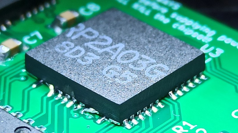
You can achieve a lot with a Dremel. For instance, apparently you can slim the original NES down into the hand-held form-factor. Both the CPU and the PPU (Picture Processing Unit) are 40-pin DIP chips, which makes NES minification a bit tricky. [Redherring32] wasn’t one to be stopped by this, however, and turned these DIP chips into QFN-style-mounted dies (Nitter) using little more than a Dremel cutting wheel. Why? To bring his TinyTendo handheld game console project to fruition, of course.
DIP chip contacts go out from the die using a web of metal pins called the leadframe. [Redherring32] cuts into that leadframe and leaves only the useful part of the chip on, with the leadframe pieces remaining as QFN-like contact pads. Then, the chip is mounted onto a tailored footprint on the TinyTendo PCB, connected to all the other components that are, thankfully, possible to acquire in SMD form nowadays.
This trick works consistently, and we’re no doubt going to see the TinyTendo being released as a standalone project soon. Just a year ago, we saw [Redherring32] cut into these chips, and wondered what the purpose could’ve been. Now, we know: it’s a logical continuation of his OpenTendo project, a mainboard reverse-engineering and redesign of the original NES, an effort no doubt appreciated by many a NES enthusiast out there. Usually, people don’t cut the actual chips down to a small size – instead, they cut into the mainboards in a practice called ‘trimming’, and this practice has brought us many miniature original-hardware-based game console builds over these years.
After cutting them to rough size, and carefully sanding the edges to get the chips to the final dimensions, they will look like this: pic.twitter.com/MTbYyHrvZ5
— Redherring32 (@redherring32) September 26, 2022


Wouldn’t it make more sense to just emulate all the logic on a FPGA? Would use less power thanks to the FPGA being built on a much more modern process even after accounting for the FPGA overhead.
People do what people do…
I quite like this approach!
It certainly is an interesting and creative approach; can’t fault the guy for having an idea and seeing, if it’ll work in practice!
Or just use/fabricate new fine NOACs (Nintendo on a chip), the chips used to create Famiclones?
https://en.wikipedia.org/wiki/Famiclone
You know, these chips that used to be built with humble 20th century technology and which don’t require FPGA’s with ~60 Billion transistors and a ~25 GHz ARM core as “assistance” to ‘faithful’ create the logic ‘in hardware’ . ;)
The NOACs coming out of China for the last 30 years are flawed and don’t recreate the NES chips accurately. A new NOAC that is accurate would be greatly appreciated all around!
I’ll manufacturer one if I get to a point where I don’t need money anymore, like if I win the lotto. I’ll hire Jeri or someone good at this stuff to design it. If I won a really big prize ($1B?) I’d also start a vacuum tube company to make some obscure ones instead of just the ones to go into guitar amps.
I think its about time to just design a flawless open-source replacement CPU/PPU.
It’s already getting prohibitively expensive to harvest original chips from NES consoles.
If you do not like people doing things just because they can or because it is a “silly” idea and no one else have done it before, maybe you ought to just look away. This is hackaday!
This is what I would classify as a nice hack. :)
An FPGA implementation is fine for emulation, but it doesn’t 100% match the real hardware. As there are always tiny details that are still unknown/undiscovered. Or even behavior that is non-deterministic.
A while back some new, previously unknown, non-deterministic behavior was found in the gameboy audio processing for example. And some consoles have multiple clocks with different clock drift, also giving non-deterministic behavior.
So, an FPGA cannot give the full authentic experience for the purists.
Uh, the point of an FPGA is that it is capable of EXACTLY replicating a chip’s functionality, on a gate-level kind of accuracy.
To be fair, that depends on the skill of the programmer and the understanding of the chip to be replicated, but the NES CPU and PPU are ALREADY 100% replicated in FPGAs, down to the line noise. You’re about five years or so behind on that point, my friend!
Links or it didn’t happen. I’ve seen people claim the same about the gameboy, where I know it’s not true. As that’s where my personal interest lays.
Not sure if they can find non-deterministic behavior, but gate level mapping of the MOS-6502 does exist:
http://www.visual6502.org/
To quote the authors: “In the summer of 2009, working from a single 6502, we exposed the silicon die, photographed its surface at high resolution and also photographed its substrate. Using these two highly detailed aligned photographs, we created vector polygon models of each of the chip’s physical components – about 20,000 of them in total for the 6502. These components form circuits in a few simple ways according to how they contact each other, so by intersecting our polygons, we were able to create a complete digital model and transistor-level simulation of the chip.”
They have several chips they’ve done this on. No updates in over a decade, though.
>an FPGA is that it is capable of EXACTLY replicating a chip’s functionality
Capable, yes, but do we know enough about the original hardware to make it happen? Even if you may THINK you got it right, how would you know for sure your “replication” is cycle accurate?
Although TBH, FPGA would be my choice too because it would probably be cheaper, and since I don’t have the skills to do what he did, safer.
You’re completely wrong, and are just parroting the same tired marketing line that folks like Analogue, Inc. *want* people to believe.
An FPGA is in NO WAY gate-level accurate. The overall width of the LUTs available in each logic element can and does mean that combinatorial logic that would take multiple individual gates on an actual silicon die can be put within one single logic element, as long as all of the inputs and outputs share a common route.
Developers on an FPGA are entirely at the mercy of whatever synthesis software they’re using, as well, as to how logic equations get coalesced. You really need to do some baseline level of research before parroting what some FPGA emulator developer with a vested interest in his Patreon tells you to believe, “my friend”.
Kinda true, but who gives a damn if the answers arrive a little early so long as they’re latched on the cycle they’re supposed to. I think it CAN be done, at least in theory.
The problem is we don’t have actual design files and masks to replicate, not so much the inability of FPGAs.
“An FPGA is in NO WAY gate-level accurate.”
Gate-level identical in common parlance means identical at the logic level. Silicon-level identical is what you’re suggesting, and it’s *definitely* not silicon-level identical, which is what you’re saying.
The “LUT width/equation combining/etc.” is all negligible compared to the fact that the FPGA *itself* is ridiculously faster silicon overall.
Uh, the point of an FPGA is that it is capable of EXACTLY replicating a chip’s functionality, on a gate-level kind of accuracy.
no the point of an fpga is to cram a but ton of customized logic into a single device and then be able to change it whenever you want… its the gamers that want to believe it replicated things down to the final nuance of the original design, cause hardware
That Non deterministic behavior sounds more like faulty hardware, or loose QC tolerances. More importantly, an unintended and atypical experience. Recreating that would be a step in the wrong direction. That’s almost like an audiophile adding skips to a FLAC file to recreate the “scratched CD” experience.
One could put the the NES chips under a microscope and perfectly recrate the design on a new ASIC using a modern process. The NES CPU/PPU do not need to be modeled behaviorally. There will be inaccuracies in the sense that modern transistors can run with far lower power consumption, but that’s a good thing. There’s no reason to go beyond that level of detail, because that is already an insane level of detail.
Not without mentioning that the NES had many component swaps and chip revisions, so I’m sure you already know the console isn’t even “accurate” to itself. They were still making Famicoms well after Y2K. There is no “pure” NES to be “purist” about.
Windows 98 games often fail to run correctly on later versions of Windows. This is due to actual bugs in Windows 98 that are not faithfully replicated in later versions of Windows. Windows 98 devs often had to work around bugs and some even exploited them to get specific desirable effects.
This applies with any system. Non-deterministic things, even if they are caused by bugs, can be very useful to game developers. If you seriously believe that not a single Nintendo dev deliberately took advantage of things like this, you don’t know how game development works. The “intended” experience is not the experience intended by the creator of the hardware. It means the experience intended by the creator of the game, and if the creator of the game took advantage of bugs and used them to create new features, trying to make a bug free simulation is going to totally lose the intent of game creator. And, it’s not going to magically restore the intent of any other game creator, because they were just as aware of any bugs that affected them and worked either around or with them to get the games they intended. Removing bugs from a legacy system like this is far more likely to break stuff than it is to fix or improve anything, because those bugs were part of the foundation the software was originally developed on.
short answer: you might or might not be correct here, but this is an awesome hack either way. might or might not be less time-consuming to go buy a Nintendo Switch, too.
Wouldn’t that be emulation, ergo may not be cycle accurate and/or 100% compatibility? At least this is still original hardware.
Yes, software an FPGA are emulation. They don’t copy the die, they implement the system in their own way through trial and error. They can be very accurate, maybe more than 99%. But to achieve higher accuracy comes with diminishing returns. 99% is good enough for most people, and especially for a commercial product. In the SNES dev scene there are constantly new demos that work perfect on a SNES console, yet have glitches on FGPA systems.
Even Nintendo’s own software emulators don’t achieve very high accuracy. Games are packaged with “tuned” versions of their emulator. It’s like the original Nintendo hardware is the original Mona Lisa, and all the software and FPGA emulators are just copies. Very close copies, but not the original (and always advertised as the original).
I don’t think there has been a gate-level reverse engineering effort of the NES’s CPU or PPU yet, or if it has, no one has published schematics for fear of the big N’s law team. Without that, a 100% accurate FPGA, ASIC, or emulator just isn’t possible for the purists.
As for this hack, while it would have been nice for this to be on chips that aren’t as rare, I think this is an interesting investigation on miniaturizing vintage hardware and cool to see that this can be done.
If some one made a fpga. Yes someone has decapped and sat there with a microscope and did the work.
Writing an FPGA based emulator wouldn’t require a decap and scan of the chip to accomplish, it would be a matter of translating a software emulator to a hardware description language. This sort of thing is done at chip companies where they go from a simulation written in something like C then build a VHDL program from that to further validate a design with FPGAs.
Followup, another commenter has pointed out that there are captures from decap and delayering efforts.
There are, but unfortunately none of the existing NES FPGA implementations are based on them.
They’re all black-box.
Better than gate:
https://www.qmtpro.com/~nes/chipimages/visual2a03/
https://www.qmtpro.com/~nes/chipimages/visual2c02/
That’s really cool. I would have thought Nintendo would try to sue such a project out of existence.
More people have dremel tools than FPGA toolchains.
Well said. I’m one of those with a Dremel but no FPGA toolchain.
https://yosyshq.net/yosys/
https://github.com/YosysHQ/nextpnr
There, now you have an FPGA toolchain. Enjoy.
There are valid arguments for me having used FPGA instead, but power consumption isn’t really one of them.
My handheld already runs 12hrs on a charge with real hardware, which I figure is way more than enough. :)
At the end of the day I wanted flawless accuracy, and I wanted to make something cool that challenged me.
I could have done it hundreds of different ways, but I’m very proud of how the method I chose turned out.
Does it make sense to make it that small? Considering that a NES Cartridge isnt that petite.
The board inside the cartridge is often tiny so if you don’t mind a bare PCB or using Famicom cartridge enclosures it can be much more compact
Nitter: Hold my Beer -> Sands down Chip in Cartridge
Judging from the photos, he has a custom small cart design as well. And NES carts where mostly empty space anyhow.
don’t need to keep the surrounding hardware identical to be accurate, could just put an FPGA or similar on the bus to act in place of the (usually pretty simple) cartridge hardware
Boo to the naysayers – this is awesome!
Took me a while to even notice the article thumbnail to be the actual thing, and not a placeholder photo.
That is awesome, fun approach! I’ve seen people trim PCBs to make stuff smaller, but not the actual CPU package. Something about seeing that 2A03 chip still used but in QFN makes me smile haha. I think the point is not being FPGA and especially not NOAC.
Have you guys though about using nitter.net links instead of twitter?
Would be better for everybody, except maybe twitter.
https://nitter.net/redherring32/status/1571606175614996480
For a site about experimenting with new ideas/methods to use stuff in unintended ways (you know … the definition of hack, which is prominently half of the site title), I’m constantly reading tons of comments questioning trying new things and how the op should’ve used conventional methods.
Agreed. There’s definitely value in following the crowd on high risk designs but if you have the resources to break things trying something new is always welcome :)
Hm. Maybe because some new ideas seem to a few readers somewhat.. Over the top? 🙂
IMHO, just because some approach is modern or highly complicated doesn’t make it automatically ingenious or elegant, too.
Personally, I’m glad that there different opinions. Constructive criticism is one of the best things out there. Because, it means that people really care about something.
The day we just stand there, smiling, clapping hands.. All together, with expressionless eyes, in total uniformity. That would be very depressing. I’m an optimist, btw.
And that’s the really important part: just because something seems modern or highly complicated doesn’t mean it should immediately be discarded and even not attempted. There’s value in learning even if the end result for the specific application isn’t practical. This isn’t about not accepting constructive criticism, but saying the equivalent of “could’ve been done with a 555” isn’t constructive … it’s only criticism and in poor form even at that.
This is truly a remarkable and beautiful approach, and a testament to how far PCB manufacturing has come in the past 20+ years. The thought that if the tech was more ahead we could’ve had this decades ago… really something!
Just shows how much space the leadframe in a dip chip wastes tiny chip surrounded by leadframe which also acts ad a heatsink neat idea
Beautifully insane!
Somebody tell Ben Heck
This is a beautiful hack. Well done.
This is the craft beer of gaming news. How many had to die before you perfected the process?