Picture showing the way the cut-down piece of chip is soldered onto the mainboard - looking, indeed, like a QFN package.

Making A Handheld NES By Turning DIP Chips Into…QFN?

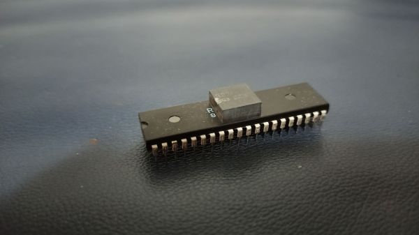
You can achieve a lot with a Dremel. For instance, apparently you can slim the original NES down into the hand-held form-factor. Both the CPU and the PPU (Picture Processing Unit) are 40-pin DIP chips, which makes NES minification a bit tricky. [Redherring32] wasn’t one to be stopped by this, however, and turned these DIP chips into QFN-style-mounted dies (Nitter) using little more than a Dremel cutting wheel. Why? To bring his TinyTendo handheld game console project to fruition, of course.

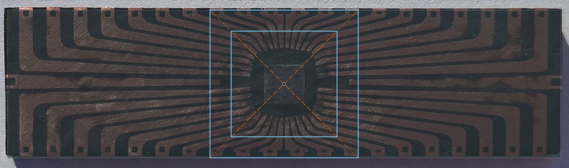
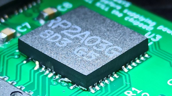
DIP chip contacts go out from the die using a web of metal pins called the leadframe. [Redherring32] cuts into that leadframe and leaves only the useful part of the chip on, with the leadframe pieces remaining as QFN-like contact pads. Then, the chip is mounted onto a tailored footprint on the TinyTendo PCB, connected to all the other components that are, thankfully, possible to acquire in SMD form nowadays.

This trick works consistently, and we’re no doubt going to see the TinyTendo being released as a standalone project soon. Just a year ago, we saw [Redherring32] cut into these chips, and wondered what the purpose could’ve been. Now, we know: it’s a logical continuation of his OpenTendo project, a mainboard reverse-engineering and redesign of the original NES, an effort no doubt appreciated by many a NES enthusiast out there. Usually, people don’t cut the actual chips down to a small size – instead, they cut into the mainboards in a practice called ‘trimming’, and this practice has brought us many miniature original-hardware-based game console builds over these years.

Continue reading “Making A Handheld NES By Turning DIP Chips Into…QFN?”

Open-DIP Surgery Cuts Retro Chips Down To Size

At least by today’s standards, some of the early chips were really, really big. They may have been revolutionary and they certainly did shrink the size of electronic devices, but integrating a 40-pin DIP into a modern design can be problematic. The solution: cut off all the extra plastic and just work with the die within.

Continue reading “Open-DIP Surgery Cuts Retro Chips Down To Size”

Deep-Sleep Problems Lead To Forensic Investigation Of Troublesome Chip

When you buy a chip, how can you be sure you’re getting what you paid for? After all, it’s just a black fleck of plastic with some leads sticking out of it, and a few laser-etched markings on it that attest to what lies within. All of that’s straightforward to fake, of course, and it’s pretty easy to tell if you’ve got a defective chip once you try it out in a circuit.

But what about off-brand chips? Those chips might be functionally similar, but still off-spec in some critical way. That was the case for [Kevin Darrah] which led to his forensic analysis of potentially counterfeit MCU chips. [Kevin] noticed that one of his ATMega328 projects was consuming way too much power in deep sleep mode — about two orders of magnitude too much. The first video below shows his initial investigation and characterization of the problem, including removal of the questionable chip from the dev board it was on and putting it onto a breakout board that should draw less than a microamp in deep sleep. Showing that it drew 100 μA instead sealed the deal — something was up with the chip.

[Kevin] then sent the potentially bogus chip off to a lab for a full forensic analysis, because of course there are companies that do this for a living. The second video below shows the external inspection, which revealed nothing conclusive, followed by an X-ray analysis. That revealed enough weirdness to warrant destructive testing, which showed the sorry truth — the die in the suspect unit was vastly different from the Atmel chip’s die.

It’s hard to say that this chip is a counterfeit; after all, Atmel may have some sort of contract with another foundry to produce MCUs. But it’s clearly an issue to keep in mind when buying bargain-basement chips, especially ones that test functionally almost-sorta in-spec. Caveat emptor.

Counterfeit parts are depressingly common, and are a subject we’ve touched on many times before. If you’d like to know more, start with a guide.

Continue reading “Deep-Sleep Problems Lead To Forensic Investigation Of Troublesome Chip”

The Dual In-Line Package And How It Got That Way

For most of human history, our inventions and innovations have been at a scale that’s literally easy to grasp. From the largest cathedral to the finest pocket watch, everything that went into our constructions has been something we could see with our own eyes and manipulate with our hands. But in the middle of the 20th century, we started making really, really small stuff: semiconductors. For the first time, we were able to create mechanisms too small to be seen with the naked eye, and too fine to handle with our comparatively huge hands. We needed a way to scale these devices up somewhat to make them useful parts. In short, they needed to be packaged.

We know that the first commercially important integrated circuits were packaged in the now-familiar dual in-line package (DIP), the little black plastic millipedes that would crawl across circuit boards for the next 50 years. As useful and versatile as the DIP was, and for as successful as the package became, its design was anything but obvious. Let’s take a look at the dual in-line package and how it got that way.

Continue reading “The Dual In-Line Package And How It Got That Way”