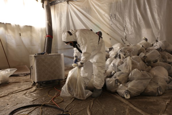
For much of the 19th and 20th century, the mining and use of asbestos saw near-constant growth, with virtually every material used in the construction of homes, offices, ships, road networks and industries featuring this miraculous mineral in some fashion. Some of these materials would contain only a few percent asbestos mineral as a binder, while others would be mostly or entirely composed out of asbestos.
What had begun as mostly a curiosity thousands of years prior was now turning into the material that was helping propel humanity into an era of hitherto unknown levels of prosperity and technological progress. It seemed as if the addition of even just a bit of asbestos would make houses weather- and fireproof, make concrete and asphalt nearly indestructible and add just that little bit of zing to tiling and interior decorations, as well as rigidity to the predecessor to today’s plastics: bakelite. Continue reading “Asbestos: The Miracle Mineral Of Our Worst Nightmares”→
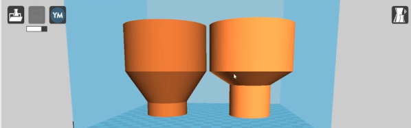
If you want to 3D print arbitrary shapes with an FDM printer, you often find you need supports. If you have dissolvable support material, that might not be a big issue, but if you use the same material for support as you print in, removing it can be difficult, depending on the location of the support and your slicer. At the very least, it is going to require more time and filament to print and at least some post-processing. [Slant 3D] asserts that you can always redesign the part using chamfers and fillets to avoid needing support to start with. Watch the video, below.
Of course, sometimes you just need to flip the part around. For example, the part in question — which is just an example — could just be rotated to avoid support, but that isn’t the point, of course. A fillet, however, still might need support, so you wind up having to do a double fillet to really avoid support.
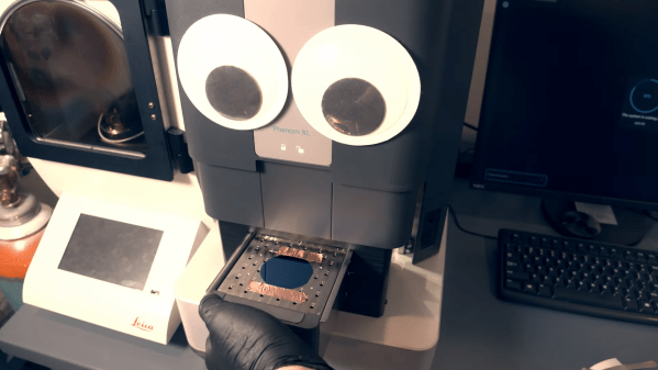
Over the past few years we’ve seen several impressive projects where people try to manufacture integrated circuits using hobbyist tools. One of the most complex parts of this process is lithography: the step in which shapes are drawn onto a silicon wafer. There are several ways to do this, all of them rather complicated, but [Zachary Tong] over at Breaking Taps has managed to make one of them work quite well. He shares the results of his electron-beam lithography experiments in his latest video (embedded below).
In e-beam lithography, or EBL, shapes are drawn onto a wafer using an electron beam in a vacuum chamber. This is a slow process compared to optical lithography, as used in mass production, but it is reasonably simple and very flexible. [Zach] decided to use his electron microscope as an e-beam litho machine; although not designed for lithography, it has the same basic components as a real EBL machine and can act as a substitute with a bit of software tweaking.
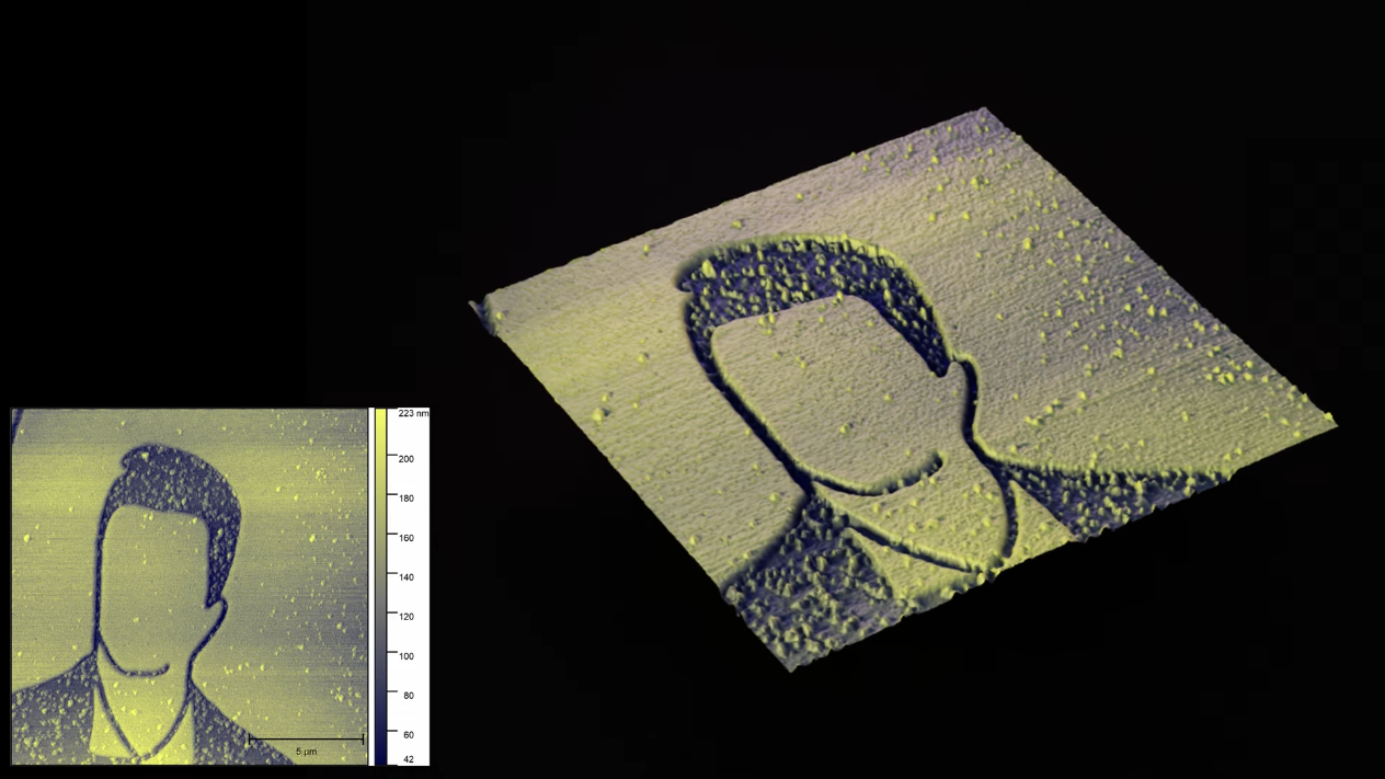
[Zach] also has an atomic force microscope, which he used to make these beautiful images.The first step is to coat a wafer with a layer of e-beam resist. [Zach] used PMMA, commonly known as acrylic plastic, and applied it using spin coating after dissolving it in anisole. He then placed the wafer into the electron microscope and used it to scan an image. The image was then developed by rinsing the wafer in cold isopropyl alcohol.
[Zach] explains the whole process in detail in his video, including how he tuned all the parameters like resist thickness, beam strength, exposure time and development time, as well as the software tricks needed to persuade the microscope to function as a litho machine. In his best runs he managed to draw lines with a width of about 100 nanometers, which is seriously impressive for such a relatively simple setup.