Aside from idle curiosity, very few of us need to see inside chips and components to diagnose a circuit. But reverse engineering is another story; being able to see what lies beneath the inscrutable epoxy blobs that protect the silicon within is a vital capability, one that might justify the expense involved in procuring an X-ray imager. But what’s to be done when such an exotic and expensive — not to mention potentially deadly — machine breaks down? Obviously, you fix it yourself!
To be fair, [Shahriar]’s Faxitron MX-20 digital X-ray microscope was only a little wonky. It still generally worked, but just took a while to snap into the kind of sharp focus that he needs to really delve into the guts of a chip. This one problem was more than enough to justify tearing into the machine, but not without first reviewing the essentials of X-ray production — a subject that we’ve given a detailed look, too — to better understand the potential hazards of a DIY repair.
With that out of the way and with the machine completely powered down, [Shahriar] got down to the repair. The engineering of the instrument is pretty impressive, as it should be for something dealing with high voltage, heavy thermal loads, and ionizing radiation. The power supply board was an obvious place to start, since electrostatically focusing an X-ray beam depends on controlling the high voltage on the cathode cup. After confirming the high-voltage module was still working, [Shahriar] homed in on a potential culprit — a DIP reed relay.
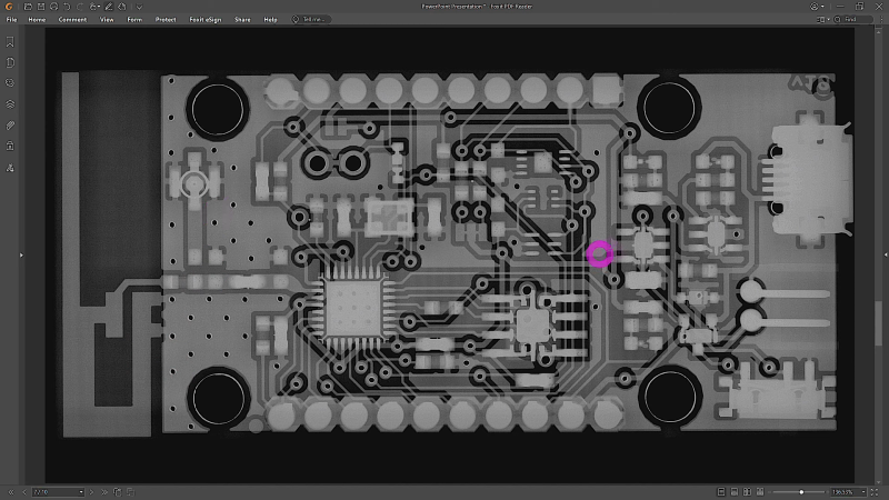
Replacing that did the trick, enough so that he was able to image the bad component with the X-ray imager. The images are amazing; you can clearly see the dual magnetic reed switches, and the focus is so sharp you can make out the wire of the coil. There are a couple of other X-ray treats, so make sure you check them out in the video below.


Just thought about that a combination of a sharp enough focus, combined with a very low depth of focus would be excellent for reverse engineering PCB’s. If you can focus on one of the internal copper layers, while the others are out of focus, then it’s easy to make a map of that single layer. A bit like a 2D CT-scan, but you make use of a shallow focus depth to skip the 3D matrix computational stuff.
Sure, to skip the reconstruction math, “all you have to do” is run the x-rays through a high-numerical-aperture lens. Difficulty: the refractive index of all ordinary matter for X-rays is approximately 1.
X-ray “optics” consist almost entirely of masks with holes. With enough agony, you can build mirrors, as long as the x-rays strike them at a VERY shallow angle. No low-F-number lenses available, unfortunately.
So only straight lines, no focusing except point sources and small holes. Maybe focusing with a funnel could work if mirrors with shallow angles work. You could at least improve efficiency over just blocking most of it with the stuff around a hole.
But if focusing does not work, then tilting still may work. By tilting either the PCB or the X-ray source you can create relative shifts of the inner PCB layers. This is also a bit closer to what a CT-scanner does.
A point source and rotating the object make constructing a 3D object pretty easy- not really any advanced math- just additions along the vector from the sensor back to the source. Lots of pictures from lots of angles- and you get a 3D representation- which is the most basic way that CT scanners work.
Exactly. In fact, SHIFTING the source and detector in a plane gives you “focal plane tomography”, which was in use before COMPUTED tomography became practical.
https://en.wikipedia.org/wiki/Focal_plane_tomography
I suspect it would still be hard to get sufficient resolution to image inner layers of a multi-layer board.
Great video! It must have felt good to be such a cheap and easy fix after some troubleshooting. If one of the voltage multipliers was suspect, since you have 3 of them, you could have also swapped between them if you didn’t have such a nice test setup.