Recently a team at Fudan University claimed to have developed a picosecond-level Flash memory device (called ‘PoX’) that has an access time of a mere 400 picoseconds. This is significantly faster than the millisecond level access times of NAND Flash memory, and more in the ballpark of DRAM, while still being non-volatile. Details on the device technology were published in Nature.
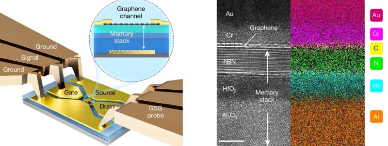
In the paper by [Yutong Xing] et al. they describe the memory device as using a two-dimensional Dirac graphene-channel Flash memory structure, with hot carrier injection for both electron and hole injection, meaning that it is capable of both writing and erasing. Dirac graphene refers to the unusual electron transport properties of typical monolayer graphene sheets.
Demonstrated was a write speed of 400 picoseconds, non-volatile storage and a 5.5 × 10⁶ cycle endurance with a programming voltage of 5 V. It are the unique properties of a Dirac material like graphene that allow these writes to occur significantly faster than in a typical silicon transistor device.
What is still unknown is how well this technology scales, its power usage, durability and manufacturability.


Fundamental research and experimental results like this are critical for developing the technology of the future, if it’s replicable. Unfortunately, not all positive results in a lab will lead to commercial viability, but the promise is intriguing.
FeRAM/FRAM won’t die either, but it merely evolved from 8KB units to 8MB units. If I’d invest, I’d bet on MRAM as NV-storage, which reportedly had 1ns already in 2008 and lasts 10E8 cycles, which is 100 more than this storage.
Some CTO might ask: Why should we care? We got UPS and on top backup batteries in the servers for the RAM.
I’m not an Intel fan, but it is sad that Optane and 3D XPoint became irrelevant. How do you market it, if your customers don’t really require it? I still have some 256K Cypress FRAM (~90ns) at home but maybe I buy some 4096K Everspin MRAM (~35ns) to play with.
If you have a low-latency constant write loop it makes for an amazing backup storage for your MCUs.
You seem have a classic blind spot around marketing, thinking perhaps that supply is governed by demand ,demand which is created by something meeting a need. Not so much , what we have now is an all encompasing advertainment industry, that if it had a moto, would be, “We can supply demand”…….”to order”, and bieng able to throw down with pico seconds when all the old nano second stuff just laggs and draggs….nobody has time for that…eh!
That, and there is a growing(real) demand for local (removable)storage.
As a user I totally demand better storage than chinese-grade flash. We had reliable casette tapes and floppies in the 80s which were in another league in terms of data durability as compared to flash, especially MLC cells (aka the Russian roulete of reads). Then I also demand better RAM without rowhammer issues. RAM in the 80s and 90s was less integrated and so it was more reliable.
And yet nobody listens to these demands. Strategic interests in shepherding people to Cloud storage might have something to do…
It will not be replicated, it will evaporate into the mist.
Yes, projects from China run a lot higher in non-repeatable results than the average 80% of scientific papers. There is a powerful tug-of-war between what the Party wants to see, and the primary directive in Chinese life, ‘avoid being noticed’.
Please fix the sentence .. “It are the unique properties …”
‘fix’ a correct sentence?
Must be hard to be an editor with such demands :)
Given the plural “These are the unique properties” could sound more fluid.
Even if production versions have significant limitations and/or very high cost (I can’t imagine this can be done via traditional deposition, so physical scale will be at the die level rather than process transistor level), this could have use as a small bootloader (faster boot time), retentive configuration registers for an MCU (again, boot time), or a subset of an instant-on FPGA’s LUTs (again again, boot time). The last might be harder as it would really disrupt the fabric layout.
“millisecond level access times of NAND Flash memory” do you mean nanosecond? I can’t imagine running Linux from millisecond NAND.
It’s more like microseconds. The cited publication compares write access times, not read.
As in writing a block? I assume a working subsystem would have fast cache like an SD card or SSD?
Is it possible to build really fast logic with this Technology? CPU and RAM on same die?
The cited write time of 400 ps is indeed very good, but it refers to a single cell. In a chip, address selection decoding will take up most of the time. If this new tech works, the speed in a system will be comparable to normal RAM, but with the advantage of non-volatility. Definitely an important step forward.