
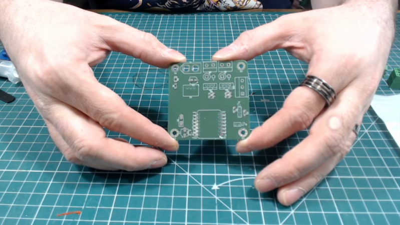
One of the extra tools someone might need when working with surface-mount components is a solder paste stencil, which not only simplifies the application of solder paste to a PCB but increases accuracy. These metal stencils can cost an annoying amount of money and take time to get delivered, so this group has developed a method to 3D print them instead.
Starting with a PCB design in one’s tool of choice, the Gerber files can be sent to the online Stenchill tool to generate the stencil. Alternatively, a KiCad plugin exists as well. The tool will output files for a 3D printer from there. An FDM printer is required, with either PLA or PETG filament, and some configuration in the slicer is needed to get the accuracy required for a useful stencil. But once that’s all set up, the printer can output a perfectly usable stencil at a fraction of the cost, and without having to wait days for delivery through the mail.
It’s not all upside, though. Although it might be better than applying solder paste with a syringe on a massive board or doing more than one smaller board by hand, it may not be as good as a metal stencil for extremely small pads. But for those who often find themselves using metal stencils and dealing with the downsides that come with them, this could be a viable alternative, especially when prototyping.
If you have a laser cutter handy, that opens up some additional options for stencil production.








Hope you’re not doing anything with a fine pitch
I think with a 0.25mm nozzle you might be able to get down to a 0.15mm wall
From the looks of things the generator has an option to merge close pads for fine-pitch, the idea being the solder paste would then wick to each pad when heated away from the solder mask
https://www.stenchill.com/en/guide
thinking about this right now, I don’t know why we don’t do this more often. We’re so concerned about the feasibility of individual fine-pitch pads when DIYing stencils; I get the feeling the consensus is just “don’t bother, just get it fabricated”. But laying down a big blob of paste and letting it wick has always been the standard way of hand-soldering fine-pitch.
I wonder if you could print it directly on the PCB? Perhaps tpu could work well.
What about simply poking holes with a needle on a film on rubber back
Ol’ Jim on the next ranch always used a pitch fork on a inner tube.
Or apply a copious layer with a builder trowel and wipe excess with a kitchen spatula, since apparently you’re after +/-1mm precision.
Thanks for the solid laugh, I’d love to see someone try.
My French just got exumed from forgotten parts of my memory. It is fun to hear how he’s trying to pronounce english words. For the young people, in 1990’s and/or 2000’s, french politics decided to replace all new tech english jargon with proper french words. Guess what a “pouce” (aka flea) is.
“pouce” is a thumb, “puce” is a flea.
I still laugh sometimes at the JT on Canal+ shtick on that one:
Le nouveau film de Mr Clint Foret de l’Est.
A resin print may be more suitable?
Hummm, have to try it, but I will check to laser cut an “rodoïd” (the plastic sheet used to protect the studends thesis…) sheet (0.02mm thick), our Trotec is very accurate.
Polyimide Film (Kapton) from McMaster has been my go-to prototyping stencil material with a 75W Epilog Legend 36EXT laser for the past ~12 years. I used 2, 4, and 5 mil depending on the design; IE: 4 mil for designs using a QFP44. The trick is not using vector cuts for the apertures which makes the most sense, but that can warp the aperture edges and interfere with a clean paste print/release. Rastering may give a less smooth edge, but the film remains very flat, so overall, better prints are achieved. I do them at 600dpi straight from GC-Prevue gerber viewing software since the Epilog Laser driver works as a printer driver.
“If you have a laser cutter handy, that opens up some additional options for stencil production.”
How about resin printers?
i’ve never worked with solder paste so myaybe it’s totally different with stencils? but i want to disclose my skill issue to correction :)
every time i have used a stencil, like with glue or latex paint or spray paint, i basically run into the problem of how to seamlessly stick the stencil to the target. like, the stencil sits 99% flat but not 100% flat, and as a result a little paint leaks out beyond the holes in the stencil. i would expect this to be way worse with FDM plastic, which always seems to have a few point Z-axis defects +/- 0.1mm?
i have come to the extreme of using masking tape as the stencil itself. in fact, laser cut masking tape would make a lot of sense to me.
is there some technique i’m missing? is solder paste just very forgiving? is it important to have a certain technique when squeegeeing the material across it?
Its not that sticky to begin with
If your print bed is very flat, you should be able to get a very good gasketing effect for paste printing. Also, solderpaste does not run like a paint or glue, it’s viscosity is significantly higher. I typically explain it as “gritty toothpaste”. When you squeegee across your stencil, the paste would only break through your gasket seal if you used way too much pressure. I use a very thin plastic putty knife and the amount of flex is what I use to gauge “proper pressure” for clean prints.
It’s a neat hack, but I don’t quite understand the motivation. Small unframed stainless steel stencils cost $3 from the usual board houses, and will be far better than anything a 3D printer can produce. They can be ordered at the same time as the PCBs, so there’s no extra delay. They’re thinner and lighter than a single PCB, so extra shipping costs are negligible.
This could be a viable technique if you’re etching your own boards, but this doesn’t seem to be the case here.
Interesting idea, I especially like the alignment corners.
There is an ever simpler solution for home made one-offs: Laser cut thick paper/thin cardboard. I have used 120g/m2 to 190g/m2 paper/cardboard with very good results for 0603 parts and TQFP packages. TSSOP works fine as well if you give up on individual cutouts for every pin but rely on the surface tension of the molten lead.
The cardboard stencil lasts long enough for a typical 5 pcs JLCPCB run, after that a mylar sheet is the better option.