Open-Source Method Makes Possible Two-Layer PCBs With Through-Plating At Home

If the last year and its supply chain problems have taught us anything, it’s the value of having a Plan B, even for something as commoditized as PCB manufacturing has become. If you’re not able to get a PCB made commercially, you might have to make one yourself, and being able to DIY a dual-layer board with plated-through vias might just be a survival skill worth learning.

Granted, [Hydrogen Time]’s open-source method, which he calls “Process 01”, is something that he has been working on for years now. And it’s quite the feat of chemistry, which may require you to climb a steep learning curve, depending on how neglected the skills from high school or college chemistry are. But for as complex as Process 01 is, it’s actually pretty straightforward, and the first video below covers it in extreme detail. It starts with a drilled double-sided copper-clad board, which after cleaning is given a bath in palladium chloride. A follow-up dunk in stannous chloride leaves a thin film of palladium metal over all surfaces, even the via walls. This then acts as a catalyst for electroless copper plating in a solution of copper sulfate, followed by an actual electroplating step to thicken the copper plating.

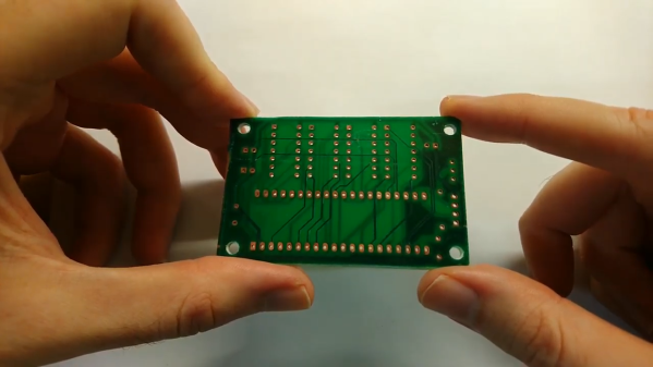
After more washing, photoresist is applied to define the traces as well as to protect the now-plated vias, the board is etched, and a solder mask layer is applied. The boards might not be mistaken for commercial PCBs, but they’re pretty darn good, and as [Hydrogen Time] states, Process 01 is only a beginning. We expect this will be improved and streamlined as time goes by.

Fair warning, though — some steps require a fume hood to be performed safely. Luckily, we’ve got that covered. Sort of.

Continue reading “Open-Source Method Makes Possible Two-Layer PCBs With Through-Plating At Home”

Printing, Plating, And Baking Makes DIY Microlattices Possible

To be honest, we originally considered throwing [Zachary Tong]’s experiments with ultralight metallic microlattices into the “Fail of the Week” bucket. But after watching the video below for a second time, it’s just not fair to call this a fail, so maybe we’ll come up with a new category — “Qualified Success of the Week”, perhaps?

[Zachary]’s foray into the strange world of microlattices began when he happened upon a 2011 paper on the subject in Science. By using a special photocurable resin, the researchers were able to use light shining through a mask with fine holes to create a plastic lattice, which was then plated with nickel using the electroless process, similar to the first half of the electroless nickel immersion gold (ENIG) process used for PCBs. After removing the resin with a concentrated base solution, the resulting microlattice is strong, stiff, and incredibly light.

Lacking access to the advanced materials and methods originally used, [Zachary] did the best he could with what he had. An SLA printer with off-the-shelf resin was used to print the skeleton using the same algorithms used in the original paper. Those actually turned out pretty decent, but rather than electroless plating, he had to go with standard electroplating after a coat of graphite paint. The plated skeletons looked great — until he tried to dissolve the resin. When chemical approaches failed, into the oven went the plated prints. Sadly, it turns out that the polymers in the resin expand when heated, which blew the plating apart. A skeleton in PLA printed on an FDM printer fared little better; when heated to drive out the plastic, it became clear that the tortuous interior of the lattice didn’t plate very well.

From aerogels to graphene, we love these DIY explorations of new and exotic materials, so hats off to [Zachary] for giving it a try in the first place.

Continue reading “Printing, Plating, And Baking Makes DIY Microlattices Possible”