Open Source Replacement For EzCAD

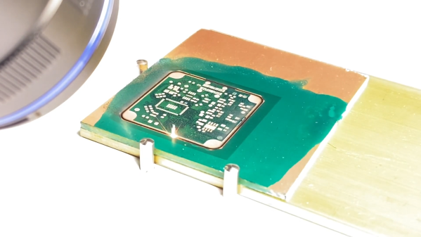
[Bryce] obtained a fiber laser engraver to use for rapid PCB prototyping last Fall. But he was soon frustrated by the limitations of the standard EzCAD software that typically comes with these and similar devices — it is proprietary, doesn’t have features aimed at PCB manufacturing, only runs on Windows, and is buggy. As one does, [Bryce] decided to ditch EzCAD and write his own tool, Balor, named after the King of the Fomorians.

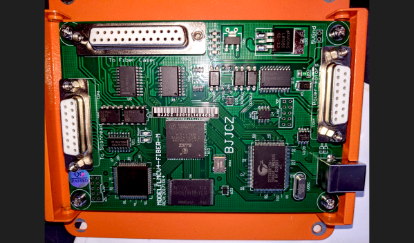
The controller board in [Bryce]’s machine is a Beijing JCZ LMCV4-FIBER-M board, containing an Altera FPGA and a Cypress 8051 USB controller. So far, he hasn’t needed to dump or modify the FPGA or 8051 code. Instead, he sorted out the commands by just observing the USB operations as generated by a copy of EzCAD running know operations. A lot of these engraving systems use this control board, but [Bryce] want’s to collect data dumps from users with different boards in order to expand the library.

Balor is written in Python and provides a set of command line tools aimed at engineering applications of your engraver, although still supporting regular laser marking as well. You can download the program from the project’s GitLab repository. He’s running it on Linux, but it should work on Mac and Windows (let him know if you have any portability issues). Check out our write-up from last year about using these lasers to make PCBs. Are you using a laser engraver to make rapid prototype boards in your shop? Tell us about your setup in the comments.

Laser Blasts Out High-Quality PCBs

With how cheap and how fast custom PCBs have gotten, it almost doesn’t make sense to roll your own anymore, especially when you factor in the messy etching steps and the less than stellar results. That’s not the only way to create a PCB, of course, and if you happen to have access to a 20-Watt fiber laser, you can get some fantastic homemade PCBs that are hard to tell from commercial boards.

Lucikly, [Saulius Lukse] of Kurokesu fame has just such a laser on hand, and with a well-tuned toolchain and a few compromises, he’s able to turn out 0.1-mm pitch PCBs in 30 minutes. The compromises include single-sided boards and no through-holes, but that should still allow for a lot of different useful designs. The process starts with Gerbers going through FlatCAM and then getting imported into EZCAD for the laser. There’s a fair bit of manual tweaking before the laser starts burning away the copper between the traces, which took about 20 passes for 0.035-mm foil on FR4. We have to admit that watching the cutting proceed in the video below is pretty cool.

Once the traces are cut, UV-curable solder resist is applied to the whole board. After curing, the board goes back to the laser for another pass to expose the pads. A final few passes with the laser turned up to 11 cuts the finished board free. We wonder why the laser isn’t used to drill holes; we understand that vias would be hard to connect to the other side, but it seems like through-hole components could be supported. Maybe that’s where [Saulius] is headed with this eventually, since there are traces that terminate in what appears to be via pads.

Whatever the goal, these boards are really slick. We usually see lasers used to remove resist prior to traditional etching, so this is a nice change.

Continue reading “Laser Blasts Out High-Quality PCBs”