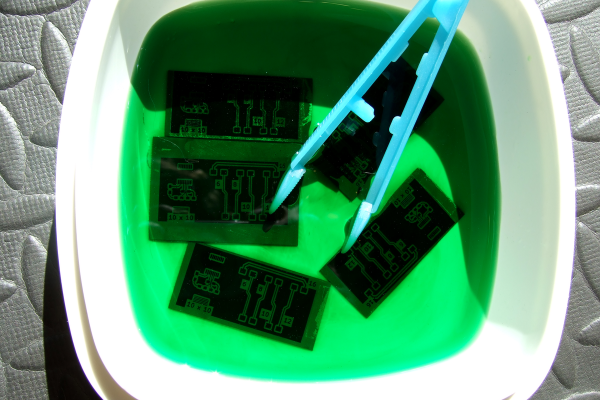
For a lot of reasons, home etching of PCBs is somewhat of a dying art. The main reason is the rise of quick-turn PCB fabrication services, of course; when you can send your Gerbers off and receive back a box with a dozen or so professionally made PCBs for a couple of bucks, why would you want to mess with etching your own?
Convenience and cost aside, there are a ton of valid reasons to spin up your own boards, ranging from not having to wait for shipping to just wanting to control the process yourself. Whichever camp you’re in, though, it pays to know what’s going on when your plain copper-clad board, adorned with your precious artwork, slips into the etching tank and becomes a printed circuit board. What exactly is going on in there to remove the copper? And how does the etching method affect the final product? Let’s take a look at a few of the more popular etching methods to understand the chemistry behind your boards.
Continue reading “Copper Be Gone: The Chemistry Behind PCB Etching”


