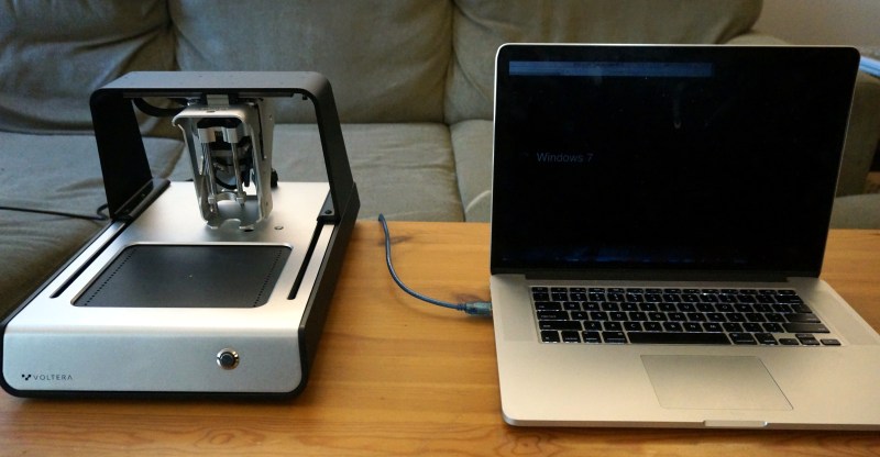
Back in Feburary, I was one of the first people to throw some cash at the Voltera V-One circuit board printer on Kickstarter. With an anticipated delivery date of Q4 2015, I sat back and waited. This week, my V-One arrived!
I’ll preface this article by pointing out that I do know the folks at Voltera as we went to university together. That being said, I did put down my own cash for the device, so I’ve bought the right to be critical. I also have no relationship with their company. In this article, we’ll go through unboxing and printing, then get into a review of the V-One based on what we’ve seen so far.
Unboxing
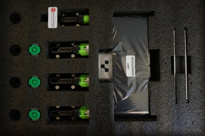
The V-One arrived in a big brown box, with its many parts secured in foam packaging. The included Quick Start Guide pointed me to the Voltera Start Page which gives step-by-step instructions on the unboxing, assembly, and setup of the printer. This mostly requires loading syringes into their holders, and installing the V-One application onto your PC.
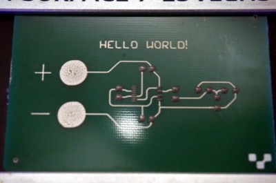
Opening the Voltera V-One app, you’re greeted with the “Hello World” circuit. Voltera ships the components for this simple board with the printer. It’s a little blinky LED design, consisting of a 555 timer, some LEDs, resistors, and a 9 volt battery.
Printing
The printing process has a number of steps, which the software guides you through. The videos included within the app are a nice addition, as they walk you through every step visually.
After clamping a blank board onto the printing bed, the printer needs to be calibrated. This process lets you tell the printer where to print, then allows it to zero the axes. It took about 2 minutes for the probe to run around the board and calibrate the Z axis.
Once the axes are calibrated, you load the conductive ink in and calibrate again. This calibration ensures that enough ink is dispersed to make continuous lines, while not causing those lines to overlap. The conductive ink is the equivalent of copper traces on a normal PCB, so the goal here is to ensure good connections and prevent short circuits.
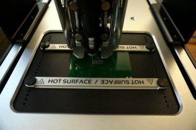
Next, the conductive ink is printed. This took about 7 minutes for the Hello World board. The machine makes some nice stepper motor sounds as it lays down conductive ink. I had some calibration issues, and ended up with traces that were not solid. I fixed this by manually placing some conductive ink onto the board. It’s clear that calibration is one of the biggest challenges of this product, and it takes some attention to make sure it’s right.
With the conductive ink on the board, it was time to bake it. This requires flipping the board over, and letting the V-One heat it up to about 220 degrees Celsius. The baking took a total of about 30 minutes, with another 10 minutes to cool off. The final step is to scrub the board with an included burnishing pad to prepare the surface for soldering.
Solder Paste Dispensing
Now that the Hello World board is printed, it was time to dispense solder paste. This is an interesting feature, because it can be used to dispense paste on any PCB, not just those made on the V-One.
You use your arrow keys to align the probe with two pads. These are used as reference points to determine the location of the other pads. The probe then moves around to determine the height of every pad. The dispenser is then loaded, and it moves around printing out paste. It did this in about a minute, and the placement was quite accurate.
Reflow
With the paste on, it’s time to break out the tweezers and place the components. Hitting the reflow button in the app automatically starts heating the bed according to the reflow profile.
The automatic setting is designed for the paste provided with the printer, but there is also a manual mode for doing your own reflow profiles. The solder paste dispensing and reflow combination is a nice alternative to solder stencils and toaster ovens.
Review
This unit is the 6th one delivered, and even had a nice “Development Unit” sticker on the packaging. I was expecting to get something pretty alpha. Overall, I’m impressed by the quality.
The unboxing and introduction material was quite good, with only a couple confusing steps. The videos clarify this and guide you through the entire process. The printer has RGB LEDs that are used gratuitously. They glow different colors for every step of the process, and pulse red when the unit is hot. The user interface is quite easy to use, which I find surprising for an early model.
The mechanical design and build quality feel solid. The frame is aluminum and has some heft to it. My only mechanical concern so far are the screw holes used to mount the board clamps. They’re tiny, and the threads might be prone to stripping. Since this is a tool that requires precise calibration, we’ll have to see how well it holds up over time.
The software is easy to use and looks nice, but did have a few issues on my PC. There is no Mac version of the software yet, though it’s expected shortly, so I opted to run in Parallels Desktop. This seems to work well, but I did have some issues with the app crashing during calibration. Once it started printing, it was stable.
One concern with any tool like this is the consumables. The ink has to be purchased from Voltera, and it’s not clear if you can manually refill the syringes. The amount of ink you get with the printer doesn’t look like much, but it’s hard to tell how much printing can be done before re-ordering. You’re also buying into the company, since you’ll need them to be around to provide consumables in the future.
Thankfully, Voltera hasn’t taken a inkjet printer approach to this. The syringes appear to be a standard type, so there’s some hope for recycling them. Fortunately, the printer works with standard FR4, so no special material is required to print onto. They haven’t baked in any DRM either.
While the V-One might look like the laser printer for PCBs, it’s not quite at that level of convenience. There are numerous steps requiring user interaction, and the total print time for a very simple board was about an hour. You need to be careful about calibration, or you’ll have continuity problems. Yes, this is much quicker than the turnaround time of a PCB fab, but it’s not instant.
Finally, there’s some obvious limitations. This isn’t a mill, so it’s only going to be able to do surface mount. The print area is only 138 mm by 102 mm (5.5″ x 4″) which will limit the size of your boards. At a price of $2199, it’s not the cheapest way to make your own PCBs, though it’s well below the price of professional PCB mills.
In Closing
Why might you want a V-One on your desk? Overall, it seems like a great tool for prototyping with surface mount components, and for doing very low volume assembly of professionally spun PCBs. It definitely will appeal to hardware startups and other companies that need prototypes assembled fast and cheap.
The folks at Voltera have managed to put out a very usable product as an on-time Kickstarter. If you want to pick one up, they’re available for preorder and shipping in 2016. We’ll keep playing with the Voltera, and keep you posted on what comes out of it.


So what is the resistivity of the trace material?
Approximately 70e-8 ohm-meters according to google.
So a 1 mil wide 1 mil thick trace would have a resistance of about 10 kOhms per meter, or about 250 ohms per inch.
Are you sure about the calculations? If true that would make that printer completely unusable for anything except printer resistors.
printed
It’s 12mOhm/sq at 70micrometer height, so R per meter is 12e-3 * 1.0/0.2e-3 ~ 60ohms/meter
It’s 12e-3ohms/sq at 70um height. So, 12e-3 * (1.0/0.2e-3) ohms / meter = 60ohms per meter
(See the voltera site for trace min width – 0.2mm, resistivity/sq – 12mOhm/sq)
Seems off by an order of magnitude. I get 27.5ohms/inch. Also, 70e-8 ohm-m seems a bit high.
http://www.wolframalpha.com/input/?i=70e-8ohm-meters+*+1inch%2F%281mil*1mil%29
I found a link for 14.5uohms-cm for solder paste.
http://www.mgchemicals.com/downloads/tds/tds-4860P.pdf
That puts it at ~6ohms/inch. Still not very good.
Dax’s number is for 1mil wide track. You have to divide down the number by the width of your track. So a 10mils wide track is 25 ohms/in which is about the right figure. Obviously 10 mils is what anyone can do with toner transfer with practices, so there isn’t much to brag about.
Also, 1 mils is 25.4 microns. If the thickness of the trace is 70 microns, then the number divides further down to about 9 ohms per inch.
The voltera ink is supposed to have 40x the resistivity of copper.
So what we’re saying is, nobody has the slightest idea what the resistance is? There’s a different number in every post, by orders of magnitude!
Would probably be easiest if Eric would be so good as to print out a few tracks and actually measure them. Particularly after baking and soldering and the like. I’m impressed this thing prints solder paste too, sounds really useful, iron the bugs out and you’ve got a 1-stop PCB machine.
Hi Andy,
The sheet resistance is 12 miliohms per square, at a height of 70um. You can find the specifications on our website.
As a rule of thumb, when using our printer you can expect a 12mil trace about 2 inches long should be about 1ohm.
Thanks for your interest! Let me know if we can help further.
Maybe you can actually demonstrate some real-world measurements on printed traces?
Your numbers do not add up. 2″ track 12 mil wide is 2000/12 = 166.7 square When you multiply by 12 milliohms/square, it gets 2 ohms per 2″. (12 get canceled) So either you are printing with height of 140um or numbers are off by factor of two.
This looks really cool; I hope this takes off like 3D printers have done. The ability to make circuit boards – right then and there, so long as you have three hours and the components – seems great. Granted, you would probably not want to manufacture on one of these things, but prototypes and one-offs would be a lot more attainable. While we’re on the 3D printing analogy: I sincerely hope that the ink and boards don’t become DRM, as some of the 3D printing companies have done. I would really appreciate it if there was a Reddit AMA or “Ask-An-Engineer”-type webcast with the developers, just to ask them about their future plans.
Compared to using perfboard/protoboard or overnighting from some professional PCB mill for $100 this seems to be quite a nice product.
However – what kind of tradeoff are you getting with using conductive ink instead of copper traces? I’m guessing too that because of the process 2 sided boards are completely out of the question.
I’ve thouht about building a CNC mill/laser cutter/engraver and it’s my understanding that you can pretty easily do PCBs with such a setup. What kind of boards does that unit use, anyway?
“The unboxing and introduction material was quite good, with only a couple confusing steps. The videos clarify this and guide you through the entire process. ”
Nevertheless I’m sure they’d appreciate feedback on what you found confusing so they could polish the documentation.
I’ll be sending them some specifics directly :)
It’s an interesting concept, but for a professional designer like me, there are too many drawbacks that would restrict design process. For now, we still etch our boards in copper in house, or use a fab for everything with more than 2 layers (and that’s pretty much every board we make these days).
One thing i would like to know, how good is the reworkability of these printed footprints? If you build proto-circuits without having an in depth design simulation and verification process, there is usually a need to optimize around some component values, remove resistors/capacitors, remove “dead” components that burnt out… Or even work on wrong/faulty traces and add some new wires… Would be nice to get someone to do a bit of typical prototype-rework and try to resolder a component 2-3 times by hand and see how well the pads stick to the boards.
Is there any provision for drilling, for through-hole parts or connectors? They talk of a 2 layer board using “sandwich a layer of insulating ink between layers of conductive inks”, which sounds like everything only on a single side. I can’t find any mention of drilling.
Their website shows a black PCB with what looks like 6 pads for a surface mount header.
http://voltera.io/images/features/print.jpg
Does this work in practice? I mean, can you solder a 6 pin gull-wing header and manage to plug and unplug an IDC socket onto it at least once or twice without ripping the printed ink off the surface?
The idea of a quickly printed PCB sounds really seductive. I make a *lot* of PCB protos, mostly through OSH Park. But as a practical matter, I can’t think of any PCB I’ve ever made that didn’t have at least some connectors and/or through holes.
At least they should add an extremely cheap ink to the printer to print silkscreen-like stuff like polarity indicators, board names/revisions, connector-identification and use that same ink draw a crosshair for mechanical pads you have to drill to mount the board somewhere. I would not want to waste any silver ink for stuff like that that does not have to be conductive. Not shure if that ink they use to isolate the traces for “multilayer” would be fitting for that task.
Yes, I think the insulating ink would work for this. It gets baked permanent when the rest of the ink is baked before pasting and reflowing.
Why not just a layer of laptop tape?
I agree w/ you – I like the idea of using this system for one off hacks, etc but there has to be a way to connect shit. I wonder if they have come up with a good way to do it without stressing the fragile ink pads.
I received this printer yesterday. Matt (the engineer that developed the nano-particle ink) delivered it personally and helped me set it up.
This printer IMO is a game changer. The ink is incredibly robust once cured and the deposition of solder paste and reflow is an awesome feature.
This company will grow and I’m sure we’ll see improvements and enhancements in the years to come (things like drilling, routing and silk screen type printing).
Paul, I think there’s a few things that can be done. One is using SMD connectors, which is what I’m planning to try first. Also, you could spin a batch of boards with through holes for connectors, and route the ink to those holes. There is a demo where they use an Arduino shield for this.
This isn’t going to be spinning your final PCB design though. Odds are, you’ll want to move to different connectors for rigidity in a lot of cases. For example, there’s no way to do board lock connectors.
I think I would glue the connectors down.
I’m now destroying my Hello World board. The ink is stronger than expected. I can’t get any of the SMD resistors off by pulling straight up on them.
I cracked off some SMD components by smashing them against the edge of a desk. This broke the solder to ink connection, and didn’t actually remove the ink from the board. I’ll be testing with a real connector soon.
I hope you recorded the destruction. Others could be able to see how hard/easy is to destroy the ink connections, which (along with trace resistance) seems to be major headache for potential users.
Apologies for a bit of hijacking but I’ve noticed a couple people commenting that do PCB Etching so i kinda have to ask how I could get in touch with either since I’ve got a project idea that’d probably do better with ‘make your own danged board’ rather than have a lot of internal cabling to a raspbrry pi.
That out of the way. Some clarification on terms would be nice. What is FR4? I’m guessing when you mention it can’t mill that means the traces are raised above the PCB instead of etched into it? How durable are the traces compared to other methods? Have you tried heating the board to, for example, 80C to see how it behaves under heat? How Newbie Friendly is this? As in ‘I want to open my own makerspace and have one of these but I don’t personally know the first thing about PCB Etching.’
Mind you I don’t have anywhere near that kind of money on me, but this seems very aimed at potential makerspace owners, and really that’d be pretty awesome. Pity you’re so limited in board size, but with some creativity that could be gotten around with projects that need larger.
Words cannot describe how glad i am for ‘no baked in DRM and ‘Standard Syringe size.’ Here’s to hoping future iterations or printers from different companies use the same type of syringe… assuming they don’t come up with a drastically better method.
Being locked into a single company is mildly worrying, but the market is young.
FR4 is standard fiberglass-resin circuit board material without the copper on top.
https://en.wikipedia.org/wiki/FR-4
Thank you.
You can only make very limited designs with the voltera printer, compared to etching (or even milling) PCBs in copper. If you really want to set up a makerspace and have a way to quickly make circuit boards, i would currently still advise people on investing into a good laser printer, UV exposure unit and a tank to etch boards. Yes, you have to organize some chemicals and materials to make boards this way, but if you have an ink-pcb-printer, you need supplys for that machine too. Depending on how much “hacking” you are willing to do to get your own etch process set up, i’d say you can get away with a few 100$ for all the supplys. If you have >1000$ to invest, you can already start to look into really nice vacuum UV exposure units and semi-professional etch tanks.
We use the stuff from Mega-UK in our company for the few simple boards we still etch in house, and so far, the machines seem to work nicely even after years of (ab)use.
Press-n-peel sheets also work fine for low volume prototyping. The cost per unit is higher, but you don’t need UV sensitive boards or UV lamps and various chemicals. Just a laser printer, a clothes-iron, and some etchant. Some prefer to use a hot laminating machine for more consistent results, and those can be had for ~$25.
Point being that buying all the chemicals and equipment for the UV system may cost you $100+, while the peel sheets cost you a dollar each – and it’s A4/Letter size so you can cut it up into halves, or tape even smaller pieces onto cardboard for printing. The economy of the UV system starts to come in around after hundreds of boards made.
If you’re a small hackerspace just starting with less than a handful of members, you might not even need to do more than a dozen boards a year.
I assume copper clad FR4 isn’t a requirement? (since you aren’t using the copper). Can you print on any material that is the approximate thickness (1-2mm) and can stand the reflow heating?
I would think so. This will make Glass PCB much easier than the process used by [CNLohr]
Can we get pictures of the results please? I’d love to see how the ‘Hello World’ circuit turned out.
there is a pic in the article
Interesting concept, but not worth it I would say. Imagine how many PCBs I could get for 2200USD (that is excluding the materials, like the ink and board)? There is a company in my city that can make prototype PCBs (2 layers with plated vias, no soldermask/silkscreen) in less than one day (if you order in the morning, you get them in the afternoon) at about 70-100USD. And if you can wait for 2 weeks or something, just order it from Itead or Oshpark and order it with fast shipping. Several PCBs at about 20-30 USD. Otherwise, investing and setting up an etching line (Cheapest laser printer you can find+homemade UV-box+etching tank+aquarium heater) is less than 300USD to make your own boards with about the same turnout time. If I’m a small startup company I don’t think it would pay off very fast.
The only thing I see the Voltera has over etching yourself is the solder paste dispenser and oven. If it could mill/drill and print silkscreen it might be another story.
Since the conductive ink PCB have very different characteristics (transmission lines impedance, DC resistance), the
prototype do not reflect what the circuit would really behave. When you are debugging a problem, is it cause by the conductive ink or bad design?
I have ordered PCB from China. The regular $11-$14 PCB takes 5 days to make and takes 3 days for $20 International DHL. Even for those cheapo proto PCB, they beats the heck out on the design rules like 6/6, vias, soldermask and can handle a few rework. If you are good with your design/layout, you only need a few minor tweak for your proto PCB to be ready for a product.
Who do you use? Every place I’ve used ends up being 2 weeks, even with express :(
Did you try the insulating ink for jumping over a trace (create a faux two layer board?)
http://voltera.io/images/features/twolayerboard.jpg
Just wondering… but d’you think you could print up on-board capacitors that way? And maybe use a squiggly trace for a resistor? Might even help reduce a component or two where applicable, as well as being a good entry for an obfuscated PCB competition. One transistor and an LED, oscillating all by itself.
I’m working on a design for this process right now :)
follow up post or maybe a hackaday.io project page? would love to see how you end up using this thing.
Interesting, but what are the advantages to cnc milling?
Cnc allows for milling throughholes, vias, the pcb shape!!!, and even stencils (it’s easy to export the relevant layers from eagle to a cad program for complex designs).
Recently, hackaday mentioned Prometheus, which seems to be a high precision PCB CNC Router.
Anyway the Prometheus kickstarter is running now: https://www.kickstarter.com/projects/zippyrobotics/prometheus-circuit-boards-in-minutes
(http://hackaday.com/2015/09/30/world-maker-faire-2015-prometheus-and-the-new-air-quality-egg/ ).
(Btw- Anyone with a cheap CNC router can achieve high quality pcbs as well… Mine doesn’t have the high precision needed for milling fine traces, therefore I typically mill my photopositive pcbs before UV and chemical development- proper alignment is fairly easy- the trick is to deburr the copper edges on the milled pcb so that the UV mask is flush during develomplent.)
The Prometheus looks like a nice machine, but the limits they have on PCB size (127x76mm) are really a killer for me. I would have expected them to extend it at least to standard EURO board size (160x100mm).
Wow – thanks, I hadn’t seen that size limit…
Was intrigued all the way till the third to last paragraph, for that a tenth of the money i could easily edit my 300 bucks 3d printer to do the same stuff.
The resistivity of the ink seems like it would be a huge issue in most low voltage circuits. 250Ω per inch (according to [Dax]) would severely alter the working characteristics of almost any kind of circuit I can think of, except perhaps the later stages of a voltage multiplier. I think most people on this site know Ohm’s Law well enough to see the same issue I do.
That’s for 1 mil wide track which this machine and a lot of board houses can’t handle anyways. You have to divide down the number by the track width. At 10 mils which is useless for modern day pin pitch, it is still 25 ohms an inch which can be an issue. On the other hand your digital signals won’t have any ringing as the long tracks would have built in damping resistors. :P It really mess up things like decoupling when you add that much of impedance. You want to be in the tens or hundred milliohms range. So it cannot be used for chips made in modern day process.
You could in theory have solder paste over the critical tracks and that could dramatically lower the resistance.
Dax calculated the resistance for 1mil thick and wide trace, what probably isn’t the case. It would be awesome it the printed could print such as thin traces, though.
On the other hand, even one or two orders of magnitude lower resistance isn’t exactly fantastic and user would have to be careful about the design.
1×1 mils is easily converted to other widths and thicknesses.
10×3 mil trace would be ~8 Ohms per inch.
Which is still very high, unfortunately…
While I have wanted to have a home PCB manufacturing shop for a number of years, I think that I have settled on the realization that doing same-day prototypes in house is not economically or practically feasible.
Yes, you can etch your own boards (I tried this a few times), but the drilling for through hole components and the lack of solder mask for SMD components is a big deal.
Yes, you can mill your own boards with a CNC (don’t have a CNC do I didn’t try this personally), but the lack of solder mask is still a problem.
Yes, you can (often) buy professional boards locally for overnight or even same day service, but this is expensive. (Perfectly fine for companies, out of reach of hobbyists).
I feel that, at least for now, using a service like Dirty PCBs or similar is the way to go. $15 for 10 5x5cm boards, including shipping, is simply amazing. Sure it takes a month to arrive, but if you plan ahead and have multiple projects on the go it is not the end of the world. If you really want to, you can spend a bit more for faster shipping (in my experience the boards are made within a few days, and shipping is the long part of the equation).
Anyway, I am still going to be watching similar devices, but I don’t see much changing for the immediate future.
Cheers
Oh, one other thought – doing two layer boards (or higher) ranges from difficult to impossible with things like this (and home etching / CNC milling). Sure you can hand make vias with rivets or similar (I have done it by soldering wire front and back), but life is too short for doing that and finding the bad connections when finished.
Did you measure the resistance of printed traces?
The solder paste dispenser is what really intrigues me. How accurate is it? I’m not looking for BGA accuracy here, but if this thing can handle laying down paste for 48-pin MCUs and 0402 components then I will be sorely tempted to pick one up.
My issue with this when I saw it on kickstarter was cost per board. If you really do need boards right now and cost is no object, it’s a great tool. but for the cost of the supplies and the printer it’s self I can have a board house make all my boards including 2 revisions for quite a long time plus end up with real copper traces, 4 layers with vias and solder mask plus vias.
It’s a 0.5 Beta and I really hope the process refines over the next few years to make it less than $1.00 per square inch with the ability to do 5mil traces plus silkscreens, etc… but right now, I just could not come up with any justification for it. Not one of my projects needs to be built right now but can wait the 3 weeks for the boards to arrive.
I agree. There are a few companies offering this sort of price point pcb. I use ITEAD, and never had a problem. 10 finished boards for around $20 just can’t be beat.
Where do you download Open Source drivers?
I fail to see the point when you can etch a similar board — or even one of much greater complexity — in about 15 minutes.
By buying the small perforated PCB boards (with the holes plated through) one could conceivably use this to make boards with vias (and places for lugs on board connectors to solder to). Some how, and I don’t know how easy/hard it would be, direct the syringe tip along side the holes, but still hitting the pads (so ink isn’t wasted down holes). That would give some two sided capability (not sure if it would work printing both sides of such a board, with the reflow and all) without drilling and swaging vias.
I bought one of these PCB-factories from http://www.diyouware.com and works really well for make “real” PCB prototypes. It can print the circuit using a laser and dry-film, then drill the vias, also dispenses the solder paste and it’s also a 3D printer. The only inconvenient I saw is that it has a small foot-print area of 70x80mm but most of my prototypes are high-density SMD boards and I can put there a lot of components.
That thing is really cool – but looks super cumbersome to use, especially for multi-layer boards.
Still an impressive project.
I can see some changes would make it less cumbersome, and they have done much of the hardwork! The device needs some sort of quick-change board carrier jig or somethign though.. Constantly realigning boards seems horrible, even with the webcam
To me using conductive ink seems a bad idea, I’d design something around bare copper PCB’s as medium, maybe photosensitive ones.
Conductive ink just has too many disadvantages in properties and cost IMHO.
But to be fair, the bare copper basis would also create myriad of issues, what with the etching and disposing of the etch material and all.
Wonderful toy – excellent review-forum! But, “Agh!”. The ‘ohms per meter’ conversation has reached the point of speculation. Please – if not too much of a hassle – make a 1 meter long spiral with a ‘as skinny as reasonable’ trace – pull out your ohmmeter – report. Better – make as many spirals as you have room for so we can get a variance figure. Best – make some spirals with traces twice as wide and see how they correlate.
OR – perhaps you could get your Voltera buddies to do it? It seems to be something people are concerned about as this machine sort of falls into the ‘too good to be true’ category. :-)
Just sayin’ – measuring is better than calculating.
A mild suggestion from an engineer’s point of view is please pick a measurement system and stick with it. Depending on what part of the world you are in “mils” can mean many different things. Engineers and builders in literally thousands of shops in the mid to eastern USA use the term short for millimeters as an example. It took a bit to work out what the mixed metric/imperial use was actually meaning when I reading discussions concerning the ink resistivity. I was thinking a 12mm trace is huge ! ;p I can completely understand why folks were getting orders of magnitude differences in calculations. “Mils” meaning millionths of an inch is unheard of in the shops I frequent including sub-micron lithography processes. What part of the world are you guys from ?
Mils means 1/1000th of an inch, the world around. It sounds similar to millimeter, which may be why you got confused. Also different from miles, which is also similar but completely unrelated.
That Would be exactly his point. Use mm and not the imperial mils; it negates confusion.
Hi Eric,
the V-one looks very nice :-)
I hav a question please: The maximum printing area of the v-one is 138x102mm.
What are the maximum sice off the FR4 Material, that you can put on the printer?
Sorry about my bad english, im from Germany.
Thanks and greetings
Udo
guys… I have bought one… and i want to return it… This thing is just terrible… The ink nozzles keep breaking and get bended because of improper initial calibration. I have calibrated 40 times… The ink cartridges have to be kept on the fridge… And so I did… After 3 hours out of fridge, there is very little ink flowing to nothing…
The first time i have printed, i was never able to reach the last stage… The solder paste keeps flowing every time in a different quantity and result is disappointing. Since then i wasn’t able to print… the ink cartridges simply do not work…
To place solder paste, you manually have to center the probe in 2 points… It takes 1 hour to center since with naked eye is almost impossible. you need a microscope
Let me say about rivets: you have to place them with tweezers… And then a hammer… You need a microscope to do that… Impossible, and they say its easy… I’m always buying all the new things… And i always get busted…
This machine does not work
OK most of these posts are from the time that the devices was initially released back in 2015; and now it is 2022 and it is a whole new world. Many of the issues and questions raised have been negated by product improvements. The device now handles 2 sided boards and has an inbuilt drill for vias. They sell both FR4 and FR1 type boards (the latter can be drilled more easily.)
I found this device online when looking for a way to fabricate multi layer boards which this device cannot handle; just 2 layers; although it is intriguing to think it might be possible to have 2 layers on each side of a double sided board. Track resistance would only be an issue for tracks handling significant current, such as 3.3V and 5V rails and Gnd/Common rails. The track resistance could cause heat generation and voltage drop. But I guess you could just print wider tracks for them; and keep them short. You could also put solder paste on the entire length of the track.
The use-case I have in mind is to produce PCB’s for Arduino style MCU applications. Custom boards containing devices such as sensors. It is thus critical importance to me that the device can handle the small silicon devices with narrow pin spacings.
Apropos: the various board manufacturers such as Adafruit produce “break out” boards containing one of the sensor chips on its own board. But the boards are an inconsistent size and if you have several you need to devise a funny looking mounting arrangement for them. It’s better to design a larger custom board containing several devices all communicating via a single I2C bus. Then it is easier to have a standardised board size and you can create a 3D printed frame to hold the board.
Now that its well past the initial kick-starter phase the device is sold at open-market prices. Its hard to justify the cost for hobbyist use at over $5000 US.. I am looking for a second-hand one. Can anyone help ?