Back in 2015 [Ben Wang] attempted to re-invent the protoboard with the Perf+. Not long afterward, some improvements (more convenient hole size and better solder mask among others) yielded an updated version which I purchased. It’s an interesting concept and after making my first board with it here are my thoughts on what it does well, what it’s like to use, and what place it might have in a workshop.
Perf+ Overview
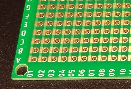
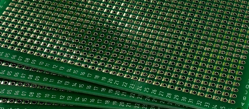
The Perf+ is two-sided perfboard with a twist. In the image to the left, each column of individual holes has a bus running alongside. Each hole can selectively connect to its adjacent bus via a solder bridge. These bus traces are independent of each other and run vertically on the side shown, and horizontally on the back.
Each individual hole is therefore isolated by default but can be connected to one, both, or neither of the bus traces on either side of the board. Since these traces run vertically on one side and horizontally on the other, any hole on the board can be connected to any other hole on the board with as few as two solder bridges and without a single jumper wire.
It’s an innovative idea, but is it a reasonable replacement for perfboard or busboard? I found out by using it to assemble a simple prototype.
Choosing a Test Project
I chose a fun idea with a low component count that I call the Laziness Defender. It is a kind of modern-day, automated Boss Key.
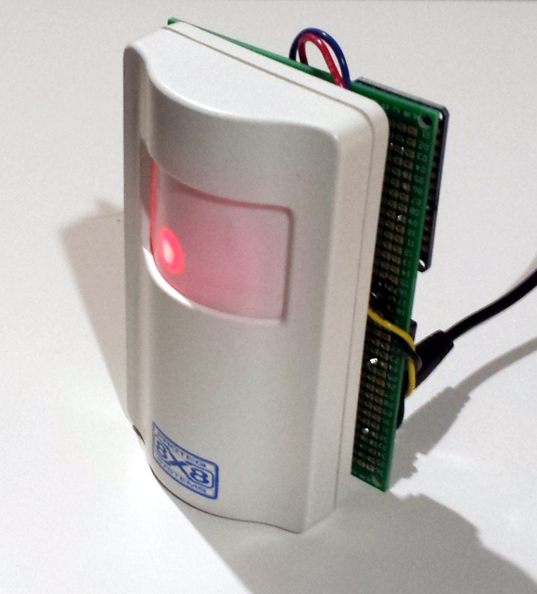
The Laziness Defender is a motion sensor that, once armed, wirelessly sends an alt-tab to a paired computer when it senses motion. A user places it anywhere within Bluetooth range, aims it towards their work area’s ingress point, presses the “arm” button, and enjoys an automatic (and silent) alt-tab to swap their solitaire game out of view the instant someone comes to invade their personal space.
No need to keep one hand hovering above alt-tab and one eye on the hallway! Being that vigilant is a lot of work, and if a person wanted work, they’d be working instead of watching videos online.
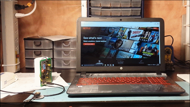
alt-tab wirelessly via Bluetooth HID when motion is sensed.Hardware Requirements
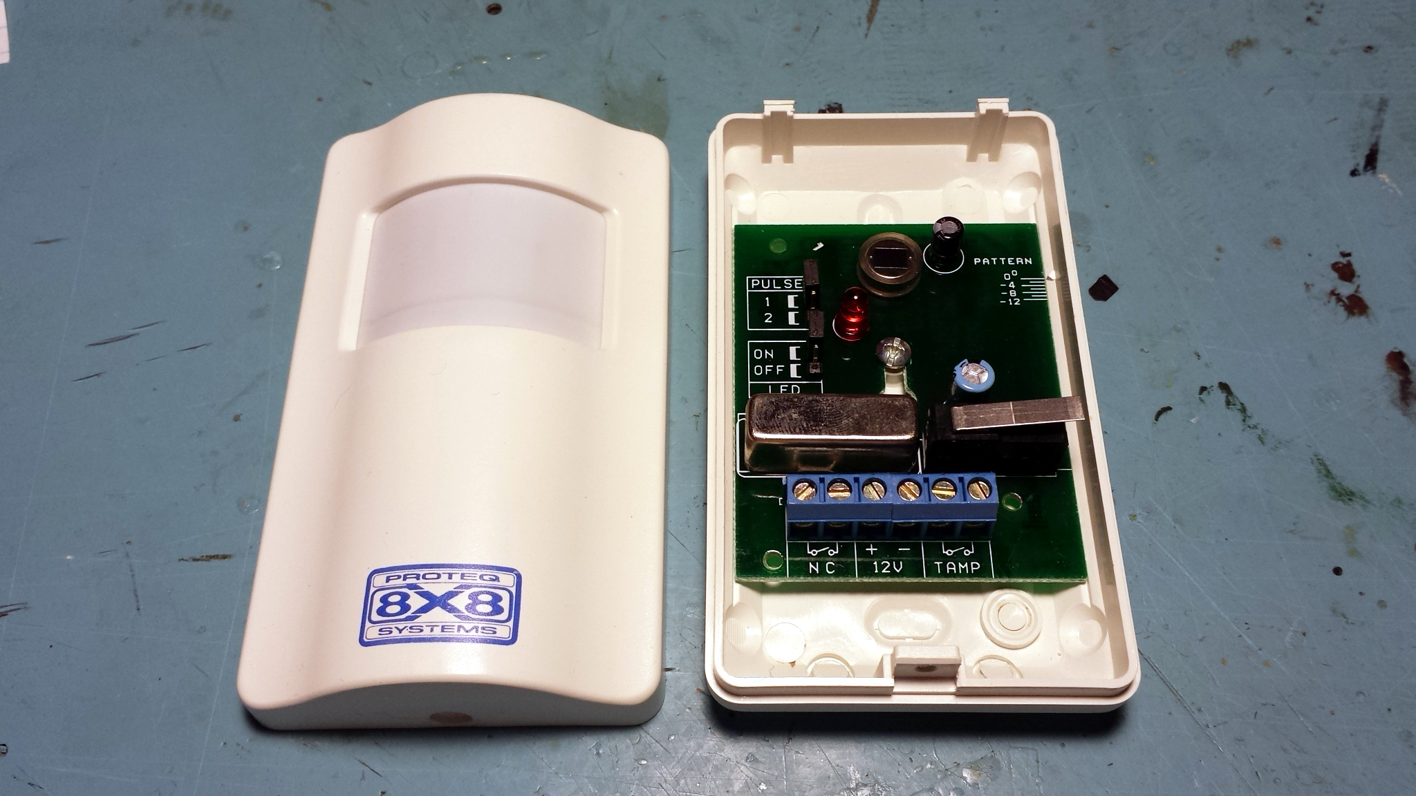
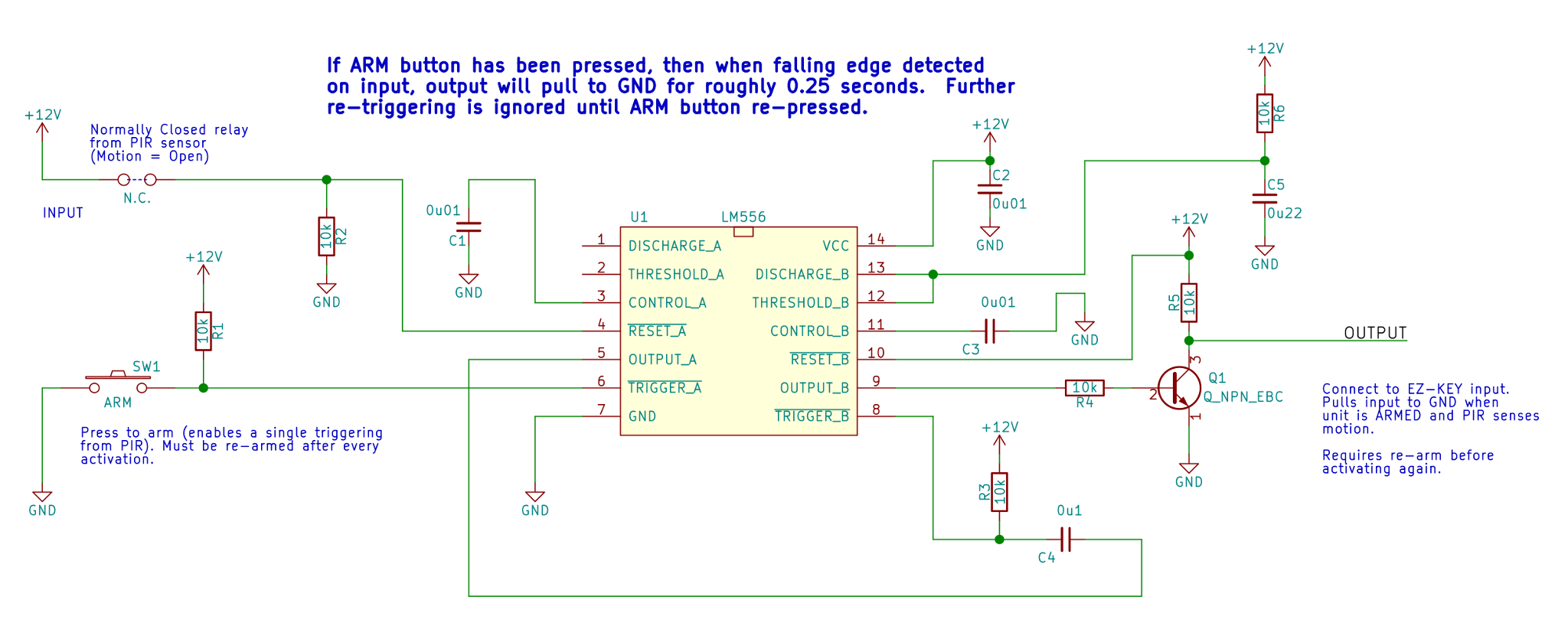
Motion sensing is handled by a surplus PIR sensor which accepts 9-12V DC and provides a normally-closed switch that opens when motion is sensed. (These are common in security systems, where the alarm is a normally closed loop that any one of the sensors can trigger by opening it.) The wireless sending of alt-tab is done with an Adafruit EZ-Key, which accepts 3-16V and acts as a Bluetooth keyboard. I configured it to send alt-tab when an input pin is pulled low.
A controller is also needed, because simply coupling the PIR sensor to the EZ-Key doesn’t do the job for two reasons: one is that the PIR sensor’s output pulse is too long; it leads to auto-repeat on the triggered keypresses. The second problem is that the unit should not send an alt-tab every time the sensor sees motion; that leads to uncontrolled behavior. The hardware must only be permitted to trigger when it has been explicitly given permission to do so. Also, to avoid having to fiddle with different voltage levels, everything should run on 9-12V DC.
If I were building this for someone who knew what an Arduino was – but not much else – then I’d probably use an Arduino to allow them to easily tweak and fine-tune the prototype’s behavior. But that’s not the case, so an LM556 will do everything that’s needed. The 556 is two 555 timers in a single DIP package. The first 555 is configured in bistable mode like a set-reset latch. This is used to let the PIR sensor trigger things only once, and require manual re-arming via an “arm” button press before it will trigger again. The other 555 is configured in monostable mode as a one-shot timer; once triggered by the PIR sensor via the first timer, it handles pulling the EZ-Key’s input low for only about a quarter of a second, avoiding the whole auto-repeat keypress issue. After triggering, nothing more happens until the “arm” button is pressed again.
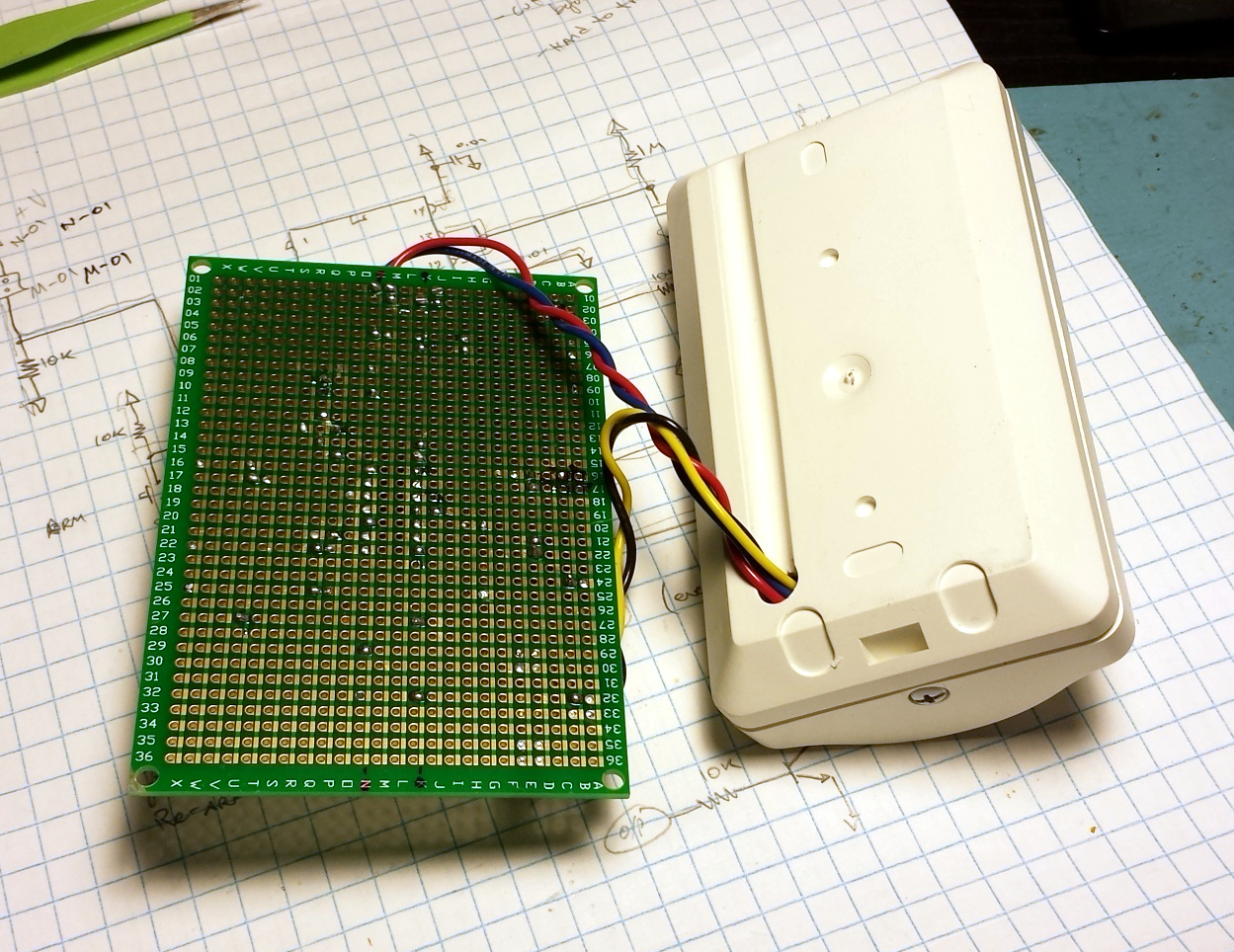
Assembly using Perf+
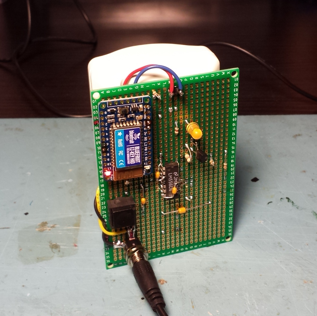
The Perf+ board was populated with:
- A 2.1mm center positive power supply plug for 9-12V input from a wall adapter
- An LM556 and a variety of capacitors and resistors (most of them 0.1uF and 10k for simplicity’s sake)
- An Adafruit EZ-Key (which acts as a Bluetooth HID keyboard)
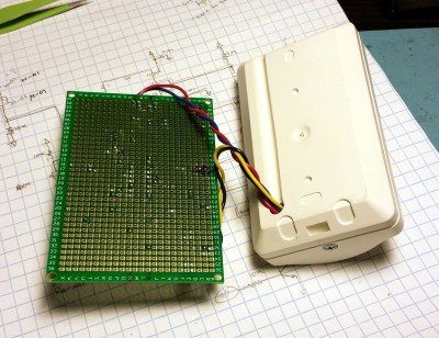
The PIR sensor is connected via 4 wires (two for power, two for the normally-closed activation switch.) The Perf+ board is mounted like a “backpack” to the PIR sensor.
The prototype Laziness Defender was assembled by diving straight in; in other words, tested on a breadboard then hacked together from the schematic like a junk-box project as though I were using normal perfboard or busboard to quickly get something working. I attempted to use the Perf+ for all the signal routing, which I did with the exception of two capacitors soldered directly to the LM556 pins because by then, I would have had to do some pretty convoluted connections to make them work and I was already running into problems keeping track of things on the Perf+ board.
There is an open-source tool called Perfy which allows visualizing and laying out connections to generate plans of where to solder, bridge, and cut on a Perf+ board, but I didn’t find it very useful for assembling a project in an ad-hoc manner.
What I Learned
-
Back of the populated Perf+ board, hardly looks used at all. Click to enlarge. The Perf+ did allow me to construct a prototype without using a single jumper wire. Wires can take up a lot of space. No wires means a smaller, cleaner looking board.
- Connections made via Perf+ are not very visual, and I found the board much harder to troubleshoot as a result. Tracing a signal’s path visually was a lot more work than it would have been with perfboard or busboard.
- Tracing a signal’s path is sometimes impaired by not being able to see underneath any installed components.
- I found it useful to mark the board for some common signals. One of the first things I did was hook up and mark the +V and GND bus lines with a marker for easy identification later. I would have appreciated a small white square of silkscreen beside the identification numbers/letters that I could color-code with a dab of a marker.
- I installed the DIP on the horizontal trace side, and I wish I had cut the horizontal traces between opposite pins under the DIP before I soldered it in, or at least installed the DIP on the vertical bus trace side. Since the pins on opposing sides of the DIP almost never need to be connected to each other, it would have made more sense to have 14 shorter bus traces (one for each pin) instead of 7 long ones across pairs of pins. Once I soldered the DIP onto the horizontal bus side, I could no longer reach the bus traces to cut them because they were under the DIP. This is one of the reasons I ended up soldering two small capacitors directly to the DIP’s leads, it was just so much easier that way. This was itself a learning point.
- Having good lighting and magnification handy was very important. I never had trouble making a solder bridge when I needed one, but my eyes are not what they used to be, and I often needed magnification to ensure that pads were only bridged where it was intended.
- Having solder wick handy to remove bridges was invaluable. Magnification was still needed to verify the bridge was completely removed.
- Excessive heat applied to one side of a hole can un-bridge a solder jumper on the opposite side.
- Whenever possible, align components to be connected directly orthogonal to one another so the connection between the two can be done with a single bus line. It’s not too bad to visually trace connections along one bus line, but as soon as you need to flip the board to follow it onto the other side it gets much harder to track.
- Cutting bus lines worked well enough with a sharp utility knife. Magnification was invaluable for confirming the trace was cleanly and completely cut.
Where Does the Perf+ Fit?
The Perf+ may have a place as an alternative to a PCB for small quantities of finished units that are not expected to need any changes or rework. The result is wire-free and clean-looking, which may be worth the added effort of planning the layout and connections with a tool like Perfy.
The Perf+ can also be used as a straightforward perfboard alternative with the added bonus of making simple bus connections very easily. Knowing when to stay away from complex routing on Perf+ in favor of the occasional jumper wire (or point-to-point soldering direct to leads) absolutely makes things easier to troubleshoot or modify later.
I love to see innovation in prototyping tools. The Perf+ and its system is simple and effective, but gives you more than enough rope to hang yourself. Making all of a board’s connections with Perf+’s built-in traces and solder bridges is possible, but even in my relatively simple board it quickly became too complex to easily follow. It makes more sense to play to Perf+’s strengths only when it clearly benefits you and your design.


Those traces get awfully close to eachother, almost enough to create a capacitor from the look of it.
Are you serious?
Welcome to hackaday,where the trolls post first.
Anyway, I mean he’s not exactly wrong, but not right either. The capacitance is almost completely negligible, and any wires of any kind form capacitors. Breadboards do have noticeable capacitance though.
Oooh, there’s something I’d never considered, I probably Havn’t done anything that’d be affected.
Anyone got a HAD fail to post about this?
This is a very real concern if you’re building a circuit for high frequency RF, i.e. GHz+. Trace shape, e.g. number and sharpness of bends, also matters.
But for anything else, who cares.
Odd, I had issues with frequencies way lower than GHz with traces/wires getting too close. In fact you can get all kinds of of seemingly unexplainable issues from it.
I had it with audio, I had it with video, and I had it in some other cases where odd behaviour was present until I cleaned things up a bit.
Now sure it’s not a 100% guaranteed issue, but if you use a board with hundreds of possible sources of such mishaps the chance would theoretically go up a bit right?
But sure, take it as trolling, see if I give a rat’s ass.
Sometimes a prototype works on the breadbord but doesn’t work when soldered since the extra capacitance works secretly as a decoupler.
The capacitance is almost completely negligible
Yeah, sure, just as those people who get themselves or others killed because of negligence.
You were right.
We have to get in before the weird stuff starts.
lol
You are correct, but if such parasitic capacitance mattered, you wouldn’t be using one of these boards anyway.
Unless you wanted the stray capacitance for someone reason. You never know.
For was thinking these boards might make for interesting directional antennas. Granted it would work better if they were all scaled to the inverse proportion of the wave and a specially made version might be better, but if you cut all the holes into U shapes and mapped the X and Y to digital pins it might be worth experimenting with. Maybe each row/column having a capacitor and inductor. Maybe stacking a dozen units with a holes spacing between them.
Thank you for using a 555 instead of an Arduino.
When I read “LM556” I thought “What a coincidence, this ATmega has the same number of the timer of my youth … wait…”
I think this was actually dreamed up from the comment section of Hackaday. Someone said, “What if” and someone else said “Why not?”. IIRC, it was a little over a year ago. I’ll try to find it when I get home tonight
That’s how I ended up building an AA battery booster to produce 3.3/5V. There was an article on SnapVCC, which dropped a 9V battery voltage to 3.3/5V. Someone asked if it would be possible to boost an AA and I already had a design laid out for a different project. I cut the booster away from the original circuit and posted it and eventually made a Kickstarter.
The non-troll comments on these articles really provide some interesting ideas.
I got the idea from sitting in a cubicle in a previous life (prototyped very badly at the time with an ATtiny25 with some library I barely understood to send the alt-tab over usb.) Honestly, it’s one of those things where there is no way it’s a unique idea. I’d love to see someone else’s take on it; they probably have a very different (and interesting) implementation.
I wonder if they could make it from some (semi) transparent material, to make it easier to follow the traces.
That would look nice. :)
Keep the leds on the inside, backlit boards.
I would have liked the solder islands a little bigger, and perhaps connected in groups of 3 on one side. That way, when placing a DIP chip, you end up with holes outside and inside the chip area that are connected to the chip’s pins, and you can use the extra traces (between the 3-hole islands) for situations where you want access from one side to the pins on the opposite side. I think that would (perhaps oddly) reduce the number of traces to cut, and would solve some of the problems that [Donald] ran into.
===Jac
This board assumes that its end user have good enough soldering skills enough to not making solder bridge. The connectivity is only in one direction, so it it very limited. Might be useful for running power/ground, but not much else.
One can do the old fashion way of soldering bare copper wires on the solder side to connect holes/pad boards like this. It take a bit of work, but offers a lot of flexibility.
http://www.zea.jp/audio/twref/2ref_409.jpg
Nice work!
BTW the picture is taken fom: http://www.zea.jp/audio/index.html Use google translate as it is in Japanese. The projects are very well documented and fine workmanship. It includes detailed theory, step by step wiring, construction techniques etc.
It looks great, though I have no idea how I personally would be able to replicate such an effort without a third limb equipped with tweezers to hold the wires in place (while using the other two for the soldering iron and the tin).
It is pretty easy. You lay down the wire first by soldering one end point. Run the wire along the path where you want it to go. You’ll need to solder down corners. You can bend the pins to hold down the wire, but it will be more difficult to remove parts later on. After laying down the wire, then you can connect the pins. If you want to, you can solder down the rest of the wire.
I train my fingers so that the last two can grab the solder or wire, so I free up a hand. For those who can’t:
https://cdn.sparkfun.com//assets/parts/2/8/5/8/09317-01.jpg
Great explanation, cheers!
There is even a video about it from that era
https://youtu.be/_ypW45Y8VSs
Actually it goes in both directions. You flip the board over and you get the other direction. you can form a via by just putting a blob in the hole and bridging both sides.
That’ll make wiring LED or keyboard matrix easy. :)
The problem with this type of board is that the wires all make electrical contact with each of the pads they traverse across. The whole point of Perf+ is that they only contact pads where you want them to, which in turn allows for much higher component density.
Maybe the right answer is to design the board wiring on a graph paper and mark where everything goes, then draw out the signal traces on the Perf+ board using colored markers to show the “wires”. The solder all the parts on and you’re done.
The open-source tool Perfy (linked in the article) does most of that planning-wise, although it’s not really a layout tool – more of a wiring/routing assist. But once you lay out the connections you can print off or display the “recipes” needed to implement it on a board – making it easier to replicate with fewer errors. If I were using the Perf+ instead of a PCB for whatever reason, I’d definitely go that route.
I really think stripboard (Verboard) is the best. Unfortunately it doesn’t seem to be popular outside the UK.
the isolated hole boards baffle me completely, seems like a barbarian way of doing things.
having horizontal on one side and vertical on the other is interesting, i haven’t seen a double sided stripboard before but i get immense satisfaction in forming neat and tidy wire links and soldering them level and without melting the insulation is a skill.
cutting traces with a sharp knife (or using the drill cutters in a hole) seems much simpler and neater than bridging links to make a track.
I used to have a pad of graph paper for designing layout with ideal sized squares but i can only find ones now with tiny squares or huge squares. a lot of the ‘cad’ is lacking also.
Hit the graph paper maker at incompetech.com You can input parameters into various styles to get what you want, then download a PDF to print as many sheets as you want. Nice and highly useful freebie.
He also does some pretty cool music, lots of Youtubers use it.
Thanks for the link. I didn’t expect the selection to be so vast. :)
I live in the US and get my mum in NZ to ship me some every couple of years :)
A few of the shops here in LA stock it, its my favorite kind of protoboard to work with!
I normally use veroboard or the neat variant with breaks in the wiring every ~5 holes that are super-handy for DIP packages. I bought a 10-pack of the Perf2 and used it to make a prototype Pi HAT. My conclusions were similar to the article, but he missed a couple of niggly points that really go to me.
You must *plan* these boards, especially where connections or cuts might be required under a larger part. You can do super-neat/compact layouts using the horizontal bars under a DIP for power lines, but it’s all got to be planned before the DIP goes in.
My biggest problem was that when you make a bridge to an empty hole, it will tend to fill the hole with solder because they’re plated-through. That becomes a real problem when you need to make a bridge on the top side of the board before installing a component – you can no longer install the component because its holes are now full! That means you either need to expand the layout a bit and use neighbouring connection bars instead of directly connecting to the component pins, or you’ll spend about 5 minutes repeatedly making a bridge, filling the hole, desoldering the hole and then discovering you’ve broken the bridge. It’s incredibly annoying.
It’s especially annoying for 2-row connectors, e.g. IDC sockets or headers. You know, the ones for connecting hard-drive cables and Pi HATs.
If you get an unexpected short under a big component, you’re f**ked. Finding where it is is super-hard, and then desoldering 40 pins from PTH? Might as well bin it.
If you solder in a big component and a bridge you made on the component side melts, you’re f**ked.
Summary: if you can get it right, Perf2 results in really neat boards with no wires (well OK, mine had one wire because I didn’t plan hard enough). However, they can be rage-inducing.
Conversely if you do a design using just passives and transistors and other little things, the boards are awesome. There was a section of my design that was just R’s and Q’s and it went in like magic. Making connections to a top-side rail with a pin on a discrete device is easy.
It’s only a problem where a package extends down to board level, e.g. IDC sockets, DIP sockets, etc.
I completely agree. AFTER you’ve installed a part is absolutely the wrong time to discover you would really really like to get at something underneath it! Luckily I never had to deal with a short or accidental bridge UNDER a part.
I also found it mildly troublesome to bridge a hole that contained a DIP pin to its adjacent bus line (i.e. one on the same side as the DIP’s body.) It’s doable but the body of the DIP makes it troublesome to get in there with the soldering iron as well as see what you’re doing. The lead on the DIP wicks up so much solder you really have to gob it on, and I feared making an unintentional bridge under there (which luckily never happened.) I much preferred making a bridge on the same hole as a DIP lead when it was on the bottom side. Easier to see what you’re doing and control things.
Thank you! Finally someone else who understands the practical aspects of using Perf+! Once a DIP component has been laid down it’s pretty much impossible to solder the pins to the “front” side because the solder bridges wind up being underneath the component itself along one side of the chip. The only alternatives are to either route traces away on the opposite side of the board (which reduces your component density) or try to apply the bridge before placing the component and face the very real and commonly-encountered issue of filling the entire pad with solder. In my experience the best way of approaching this is to 1) use a good-quality SMD soldering iron in conjunction with a magnifying glass, 2) place a tiny sliver of heat shrink in the pad hole itself while making your bridges to stop it filling with solder which you can then easily remove, and 3) keep your solder wick on hand regardless. I really do believe that Perf+ is a unique and revolutionary design that solves many of the problems of conventional breadboard design but it does introduce a new set of challenges of its own, particularly when you use it for more complex circuits.
Would like to see a variation with a ground net on the bottom and buss-bars on the top. Would need more jumper wires, but the ground net would allow easy prototyping of high speed circuits. And ground connects to EVERYTHING, so you’d still get a useful reduction in labor placing jumper wires.
Look like nice, practical board. It remind a bit of the flower perf board from I do not recall which company. Too bad the batch I had received didn’t seem to solder good. Only issue is, I’m not paying that kind of price for perf board when I can get pretty decent one in bulk for next to nothing on ebay.
I remember the flower perf board! Seemed like a great idea, but when I tried one I just couldn’t get it to work like it seemed it should. The holes kept sucking away all the solder and it felt impossible to actually bridge anything.
For anyone not familiar, it was basically a perfboard but each hole had – instead of a circular bit of copper – a flower-shaped one. The idea was that you could just bridge adjacent ones to make “traces” easily. As a side benefit, it made soldering surface mount easier (in theory). Like I said though, I tried but couldn’t really get it to bridge the way it was supposed to.
From the responses here, it seems like the next iteration would benefit from a few key points:
1: thermal relief on the pad to net connections to reduce the likelihood of disconnecting one side while soldering the other. A “neck” in the connect pad would help. Also makes it easy to cut the net rather than desoldering a mistaken connection.
2: a layout with similarity to breadboards and other perf boards. I envision the middle of the board divided in half, with power rails down the middle, chips straddling the rails and left and right side crossbar networks.
Wrapped around the edges would be a crossbar network that extends the full length and width so you can connect left and right side nets.
I raised concern with the first issue myself when the project was originally featured here, I’ve done several thousand solders on Perf+ since and I’ve never once encountered it. I have had problems connecting a non-occupied pad to a strip without accidentally filling the whole thing with solder (thus making it impossible to add a component later) but that issue has been greatly improved with the latest board iteration.
The second idea is interesting but I think it would have to be restricted to the perimeter. Spend even a few minutes designing a circuit with my Perfy editor and you’ll quickly discover that you need as many available rails on both sides of the board as possible in order to route IC connections to wherever they need to go. And if your particular circuit does need power rails down the centre well, just use a couple of regular traces…that’s what they’re for!
I think it’s pretty useful, as long as you know when to use it, and I think the article describes that pretty well. I often prototype on Veroboard and that’s what ends up in the project because the next step would be a PCB and I don’t want to go to that trouble for a one-off. This is a pretty good middle ground.
Developing windows-only program in 2016 is just a joke!
There is a new layout, https://www.kickstarter.com/projects/knivd/routaboard-the-prototyping-board I thought it was cool and I am a backer. But reading this article and looking at the new design, I can see similar problems. Anyone else a backer?
Interesting. I’m not a backer myself, but my initial impression is that in a real-world circuit this one will require a huge number of solder points to run traces around the board. One thing I did learn from working with Perf+ is that it’s an order of magnitude easier to cut a trace than it is to solder a bridge, I can’t help but wonder if they should have just kept all the nodes connected and made you cut the relevant traces away?
Any word of an SMD variant on this idea? seems like it would be mighty useful, especially if it had a ground plane on the bottom (RF project fun!)
Would you be interested in evaluating RoutaBoard as well? http://routaboard.com
Funny you should mention it, I mashed BUY on that one as well. Can’t wait to see what it does!
Has anybody seen software for the ALio ?
https://www.crowdsupply.com/aerd/alio-proto-board
Dang! These are no longer available!