In the last episode, we put our circuit boards through the reflow process. Unfortunately, it’s not 100% accurate, and there are often problems that can occur that need to be detected and fixed. That’s what the inspection step is for. One could insert an inspection step after paste, after placement, and after reflow, but the first two are icing on the cake — the phase where most mistakes can be caught is after reflow.
There are a number of problems typical with a surface mount reflow process:
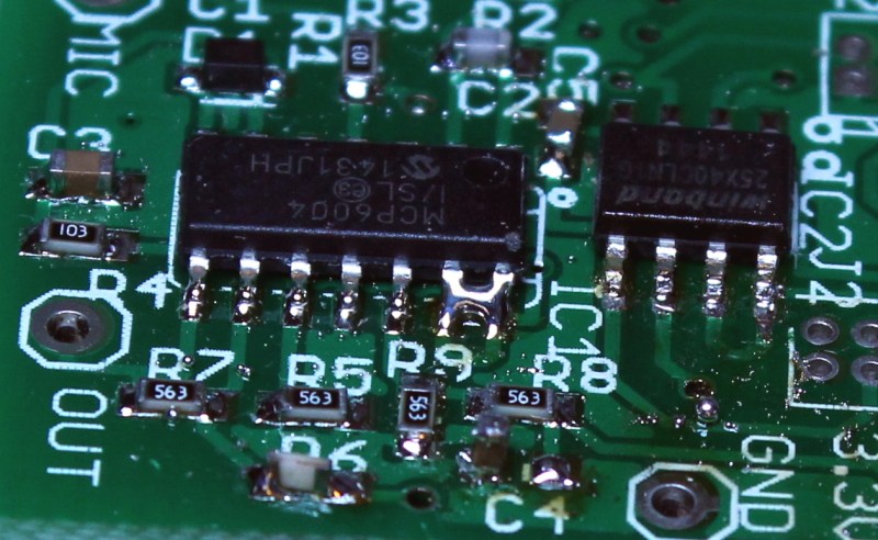
- Tombstoning – This is when a component stands up vertically. This is bad because it means the component is not connected and there is an open circuit.
- Billboarding – This is when the component flips on its side. It’s still connected, so nothing is technically wrong here, but it’s not great and could indicate other problems with the process.
- Bridging – This is really bad. When too much solder (or bad solder mask) allows for two nearby pads to be accidentally bridged with solder, creating an unwanted connection.
- Insufficient Fill – If not enough solder paste is deposited in the screen, then it may not be enough to make a connection. This is more common with QFN parts that have super tiny apertures that could get clogged, and it’s really hard to see when inspecting.
- Voiding – Similar to insufficient fill, this is when there is not solder where there should be. This could be caused by flux that has turned to gas but hasn’t had a chance to escape, leading to holes inside the joint. Or if there is a via in a pad, the solder might wick into the via creating an empty space between the pad and the intended connection.
- Spattering – Imagine a small droplet of water inside the solder paste. As the water turns to steam, it explosively releases its pressure, throwing particles of solder all over. Flux can do this, too.
- Solder Balls – Too much solder paste is applied and ends up collecting on top of some solder mask. Because the solder doesn’t stick to solder mask and instead sticks to itself, it forms little balls on top of the PCB. These balls can move around and accidentally bridge connections.
In the picture above are examples of tombstoning (C4), billboarding (R6), bridging (IC1), spattering (all over), solder balls (bottom right), and insufficient fill (IC2).
So how do we detect and correct these problems?
Visual Inspection
In the lowest volumes, usually by the person who did the assembly, the best way is to use your plain old eyeballs. A single glance isn’t nearly enough, though. It’s important to methodically look at and consciously think about each connection and whether it is good or not. Lots of good light makes the job easier, too.
Microscope Inspection
 It can be straining on the eyes to look closely at every joint, and depending on available lighting conditions and the size of the components used, it may not even be possible. Sometimes it’s necessary to bring in a microscope. You can start with a loupe, a simple handheld lens usually used by jewelers, or the magnifying glass on your helping hands. These can have built in lights as well. Then there are USB microscopes that let you see the zoomed image on a big screen. Others are purely optical and make you stuff your face up close to the eyepiece.
In Circuit Tests
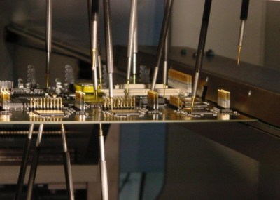
Move two probes to specific locations and measure the resistance or capacitance, and do this repeatedly, and you have a decent way of verifying the circuit. There are two variations on this. In-circuit tests use a test jig with a whole bunch of pogo pins (called “bed of nails”). The jig is pressed down onto the PCB, measurements are made from each of the pins, and it’s done. The downside to this method is the need for a new fixture when changing designs, but the upside is super-fast testing and the ability to do other operations, including programming.
The other variation is flying-probe testing, in which the machines have a few probes on a gantry that can fly around a board at dizzying speed. There is no fixture required, so setting up this testing process is much quicker and more robust, but because the process is serial instead of parallel like the ICT method, it can take longer to test each PCB, making it more expensive (plus the machines are fancy and expensive).
X-Rays and Saws
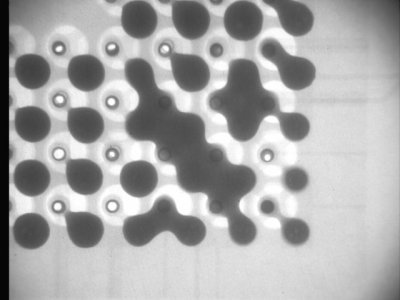
How do you know if your BGA chip was assembled properly? Zap it with some X-rays and look inside! Granted, this is not a method that’s easily available to the hobbyist, at least not without calling in a few favors, but it’s the only non-destructive way to inspect a PCB.
The other way is to slice through very carefully with a saw to take a peek. Of course, this is destructive, so it’s only good for diagnostics on the process and not the individual boards.
Cheap AOI
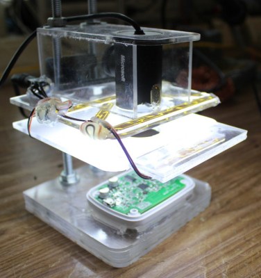
I have to mention this one because I successfully implemented a cheap AOI for production. The idea is to use a cheap webcam and OpenCV to identify faults. AOI stands for Automated Optical Inspection, and is very common for testing circuit boards. This cheap AOI is the same idea, but with a lot of limitations. Essentially, you start with a fixture that holds the PCB in place, and a webcam positioned above it so that the PCB takes up the entirety of the camera’s view. You put a few “golden” boards in and train OpenCV with templates of what the connections should look like. Then you mask out everything that’s not a component, and start running boards. A connection that matches the template will mask out on the screen, and one that doesn’t will be visible and zoomed in, making inspection easier for the operator. This method identifies bridges, tombstones, missing parts, and billboards, but there are other types of errors it can’t catch, and it’s also limited to small PCBs, with frequent false positives. Still, this method can be super cheap for what it is, so it’s good for a run of a few hundred to thousands.
Commercial AOI
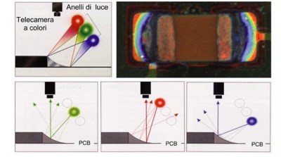
A commercial AOI is super fancy. It will have RGB leds so that it can rapidly switch between them to see where the light is reflecting and determine the quality of the solder joint based on how the light is reflecting.
The camera or PCB will be on a gantry so that the camera can focus on different parts of the board, and the AOI is trained to look for lots of different kinds of faults. They still have a lot of false positives, so it’s important to have an experienced operator that can verify the faults. This slows down the process and increases the cost, but on some boards, this is a necessary step for each board.
Functional Testing
There’s another option, and it’s the equivalent of “let’s plug it in and see if it blows up.” While a little dramatic, this is a legitimate testing solution, provided you have adequate protection on the test equipment. If it powers on, that’s a decent first step. If it can be programmed, that indicates that a lot of other hardware is running. If your firmware is clever enough, it can perform a power-on self test and read voltage levels on specific ADC pins, verify expected GPIO values, or if hooked up to USB or some other communication, report out whether it works or not. I had a project that went through a microphone calibration step, which not only verified that the microphone circuit was working, but also checked that the other sensors and LEDs were working through a series of self tests accomplished automatically in a small box, and reported over USB along with the MAC address of the device. The hardware couldn’t leave the building unless it passed every test.
Conclusion
In the end, most of these testing methods will be used for a product. In the prototyping stage, it will be visual and microscope inspection. Then flying-probe or AOI as volumes increase, with ICT coming in after the design is solidified and volumes are higher. There will be the occasional X-ray or sawing to verify that the production line is still running properly. And functional testing will almost certainly be a last stop on any production line.


AOI is definitely something to have. My CM even made a video of their line during assembly of my product:
https://www.youtube.com/watch?v=Z5d9kGRiQ-s
Nice ! Viewing it, I thought every job and business deserves its own glorious music video :)
Please could you tell us which factory this is ? (I’m in France too)
Sure: http://www.reseau-gesat.com/Gesat/Bas-Rhin,67/Illkirch-Graffenstaden,27104/apf-entreprises-alsace,e1320/
Merci !
Absolutely! I want that too, more industries, more glorious music videos!
An important problem is missing from the list: insufficient heat. It happened to me several times with small batches from professional assembly companies.
I have seen that as well. The component pins are just sitting in un-reflowed solder paste. It may even work for a while…
the first photo shows solder balls everywhere on the pcb due to poor solder paste quality, not fine enough … the short would have been non existent, heat and flux are very important too, we had those problems on our smt line production
I took a PCB and inserted all those problems for the photo because I was trying to demonstrate what each of those issues looks like without a separate photo for each. It would be pretty impressive to get all those issues in such a small area organically.
Now I know who did that to my boards! I knew the faults didn’t appear by themselves. Arrrgh!
Seriously though, a very helpful article. Perhaps somebody has a particular inexpensive solder paste to recommend? I hope there’s something above the MECHANIC branded paste sold on eBay.
Another test we had long ago that might surprise a lot of people that carry smart phones around like a box of eggs – was the meter test. Drop it from a meter on a hard flat floor and it should still be functional and not damaged. Most modern devices wouldn’t pass that test now.
I love the tip about the three colors of like for AOI. I will definitely be making on of those for manual inspection.
I love the tip about the three colors of light …
Good article, I was just looking for something like
http://bobbaddeley.com/2015/12/creating-an-automated-optical-inspector-for-50/
Thank you!
Nice article. What i’m kind of missing here is the conclusion that you need to plan ahead in your schematic design (and the layout too) for all the testing and inspection you might have to do later on. For example, if you want to do in circuit testing, don’t forget to add test points (preferrably all on one side of the board) on every important net you might need to measure later on. At the same time, for optical inspection, you have to make shure that large components don’t hide the smaller ones from the light and camera.
Adding all the testpoints and component clearances as early as possible in the design stage is important as this could influence the size of your board and have some effects on the EMI/EMC performance of the circuit too.
Zero mention of active and semi-active (high-Z) boundary-scan inspection/verification methods.