[Ken Shirriff] has seen the insides of more integrated circuits than most people have seen bellybuttons. (This is an exaggeration.) But the point is, where we see a crazy jumble of circuitry, [Ken] sees a riddle to be solved, and he’s got a method that guides him through the madness.
In his talk at the 2016 Hackaday SuperConference, [Ken] stepped the audience through a number of famous chips, showing how he approaches them and how you could do the same if you wanted to, or needed to. Reading an IC from a photo is not for the faint of heart, but with a little perseverance, it can give you the keys to the kingdom. We’re stoked that [Ken] shared his methods with us, and gave us some deeper insight into a handful of classic silicon, from the Z80 processor to the 555 timer and LM7805 voltage regulator, and beyond.
Dive In: The Z80
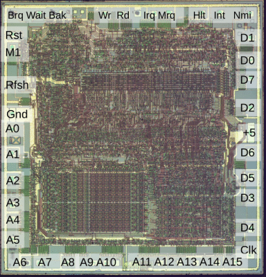 [Ken] wastes no time and dives straight into a die shot of the Z80 8-bit CPU. He starts out by labeling the landing pads that connect to external pins by cross-referencing them with the datasheet. That tells you a lot — you know what the pins have to do, so it makes guessing use for each clusters of transistors a lot easier.
When you see a bunch of repeated tiny circuits, you’re probably looking at memory. Since the Z80 has sixteen registers in its CPU, [Ken] goes looking for sixteen repeating blocks of storage, and finds ’em (lower-left). Since they’re connected up to the address lines on the pin-pads, he’s doubly-confirming his hunch. The other side of the registers heads off to a data bus, another giveaway.
The command decoder turns out to be a programmable logic array (PLA) that takes a bit pattern in across horizontal wires, matches it, and then sends a logic high down a vertical line that leads to the Arithmetic-Logic Unit (ALU). Particular to the Z80, [Ken] notes that although it takes eight-bit instructions, it’s only four bits wide. It turns out the CPU memory-speed constrained, so they saved space (and money) by using a four-bit ALU. Sneaky!
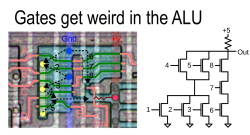 Once he’s figured out the broad outlines of the chip, it’s time to dig down into the transistors. After a brief intro to designing logic circuits out of transistors, he takes us into the actual fabric of the IC. As if things weren’t confusing enough with simple logic gates like NAND and NOR, it turns out that the designers of the Z80 used a few “crazy gates” that efficiently compute particular operations that they needed.
The ALU is the heart of a chip, and it’s highly optimized. For instance, the Z80’s ALU is “totally different” from the 6502. An adder is not just an adder. And it’s here in the ALU that you’ll find crazy gates and chip-specific implementations. Figuring out how all that works is the next level up for budding chip-reading detectives. [Ken] has a lot more on the Z80 on his website.
Clever Calculators and Forgotten Memories
The Sinclair Scientific Calculator from 1974 was a small marvel: it took a TI chip from a simple calculator “that could barely multiply” and added on logs and trig functions. How did Sinclair do it? [Ken] wanted to find out — we still hold this as one of our most favorite hacks.
Starting off again with the pinout, [Ken] finds his way to the instruction ROM. He built a software simulator for what he found, and got to reverse-engineering. Again, if you’re into clever space-saving algorithms, head on over to his website.
In 1970, RAM storage was incredibly expensive. Intel came out with “shift-register” memory, and indeed, it’s just a 512-bit-long shift register. How does random access work in this context? You wait until your bit comes around like you would on a baggage carousel — leading to slow and random random-access times. Cool. But we can also see why they went out of favor.
Analog ICs: the 555 timer, the LM741, and the LM7805
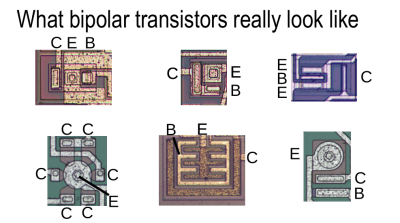 Have you ever used a 555 timer? Want to see how it works? First, you’ll have to understand the implementation details of the bipolar-junction transistors (BJTs). Although BJTs are laid-out in many more different topologies than their FET cousins, analog circuits are often smaller and easier to get your head around. [Ken] gives you a good head start, and then starts off reversing two iconic chips: the 555 timer and the LM741 op-amp.
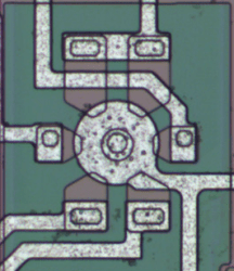 The 741 IC is dominated by an in-silicon capacitor, which really is a silly idea, but since “engineers are lazy” and this means that they have one less piece to lay out, it turned out to be worth its weight in gold and the LM741 sold bazillions. On the other hand, it’s got current mirrors spread around everywhere, which are used to replace resistors in silicon. And it’s got some strange transistors, one of which has six (!) collectors because the designers needed six current mirrors in one place.
Finally, [Ken] takes apart the LM7805 voltage regulator. The output transistor is (not surprisingly) about half of the IC die — the 7805 needs to push some current. The coolest part of the chip is a variable resistor that sets the output voltage. It’s a simple trick that makes the difference between an LM7812 and an LM7805 no more than the value of the resistor inside, leveraging the same design for different operating voltages.
How Does He Do It?
[Ken] uses a metallurgical microscope that shines its light from above, rather than through the sample. He got his for a few hundred dollars on eBay. He then takes multiple images from different locations all around the chip, with significant overlap, and lets the Hugin software stitch it all back together for him.
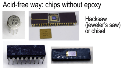 “The experts” decap their chips using boiling sulfuric or nitric acid. [Ken] doesn’t need a Superfund site, so he often leaves the die photos to someone else. Sites like zeptobars.com, visual6502, and siliconpr0n have a ton of chips that are just waiting for you to start decoding, with no chemistry degree needed.
For chips that aren’t in epoxy, [Ken] opens them by himself either by hitting them with a chisel or cutting open with a saw. He’s just now started up on the 8008 CPU. Between this talk and the resources on [Ken]’s website, you’ve got a good head start. All that’s left to do is the good, hard, fun work of puzzling out a few ICs on your own.


The intro is so cool
At work we’ve decapped using a cigarette lighter and a milling machine. Neither is pretty but both remove a lot of material in a hurry.
Does it really make sense to slag an integrated circuit for being, well, integrated? The capacitor on the 741 is 25pF. Nowadays you can get that with half a nanohenry or so of parasitic inductance if you use an 0201 part and good layout practices. In 1968? Probably two orders of magnitude higher once you consider lead parasitics on the IC and cap, not to mention the layout. And it would be *much* lower Q than an on-die part. That leads to incredibly poor, highly variable loop compensation. Not conducive to a very robust design, which is what an integrated circuit hoped to facilitate. No IC designer burns silicon for fun, every bit of die area is scrutinized and must be defended in multiple design reviews. There’s no way that capacitor is there simply to accommodate laziness on the part of the customer.
“There’s no way that capacitor is there simply to accommodate laziness on the part of the customer.”
The the Arduino came and customers started wasting million of transistors to do simple things. Compared to that, a capacitor seems nothing.
I mean, sure I could use a $5 8-bit MCU, write out a few hundred lines of boilerplate, implement a whole USB stack, write my 5 lines of actual application logic, flash it all with a $500 programmer, and then solder it onto some stripboard with voltage regulators, level shifters, resistors, and capacitors, then write USB drivers for every OS I want to work with and install those drivers on every PC I need to plug it into.
…or I could use a $5 Arduino and have something working in less than an hour.
It’s not about being lazy, and those transistors aren’t “wasted”. It’s about putting together a solution in a day instead of a month. Some of us have jobs and can’t devote weeks to building a gadget. I have thee jobs and can devote all of maybe 4 hours/week at my workbench.
When I’m designing a commercial product, I am more efficient in my choice of components and I do use the smallest MCU suitable, write crap-tons of boilerplate, and flash the MCU with a $500 programmer. When I’m trying to make my TV’s remote control Plex, I’m not going to spend more than $10 and 2 hours getting it to work so an Arduino is a perfect fit. Sure I COULD use a PIC or even a bunch of 555s, and yes I’m using a recycled IR receiver with integrated pullup and filter cap which I could build myself, but my time is a bit more valuable than that.
Yup. The transistors on an IC aren’t valuable any more. People “waste” billions of them playing Pokemon or posting nonsense on web forums. If it costs a couple of quid, and does exactly what you want, it makes sense to use an MCU over a dedicated chip. Who’s supposed to be keeping count of these “wasted” transistors?
Same way it’s not worth repairing TVs and radios any more. Technology has advanced enough, that things formerly rare and valuable are now disposable. And that generally makes life better! Hooray!
It would be nice if someone made an application that applied some CV to microscope video streams to create perfect die shots and then further processed the image into simple bitmap images of each layer. Kind of a niche software but it would make it much easier for people just starting to RE old ICs.
Maybe even make a 3D model out of it?
Fascinating talk. I never heard of “shift register memory” but it makes sense as an interim technology before manufacturing techniques advanced far enough to make RAM affordable. The first thing like it that popped in my mind was magnetic bubble memory, followed by “delay-line memory”, and CCD’s which all sequential-access electronic memory devices.
Those links will be very useful. Also chip photos have a beauty all their own. Some even resemble a top-down city.
“resemble a top-down city”
It shouldn’t surprise you to know that a part of VLSI design emphasizes “Manhattan Based Design Rules”. By restricting the chip geometries to only rectangles composed of horizontal and vertical lines, the layout software is greatly simplified. Design Rule Checkers are also much simpler for “Manhattan” designs than for designs with random shaped polygons, circles, and lines at arbitrary angles.
Awesome!
really enjoyed this talk, I get a kick out of knowing how hardcore some people are! reverse engineering die photos as a hobby! I liked playing with the 555 interactive viewer – nice work, makes it much easier to understand what’s happening. Cool music and graphics at the end of the vid too!