Gisselquist Technology recently posted a good blog article about metastability and common solutions. If you are trying to learn FPGAs, you’ll want to read it. If you know a lot about FPGAs already, you might still pick up some interesting tidbits in the post.
Don’t let the word metastability scare you. It is just a fancy way of saying that a flip flop can go crazy if the inputs are not stable for a certain amount of time before the clock edge and remain stable for a certain amount of time after the clock edge. These times are the setup and hold times, respectively.
Normally, your design tool will warn you about possible problems if you are using a single clock. However, any time your design generates a signal with one clock and then uses it somewhere with another clock, metastability is a possible problem. Even if you only have one clock, any inputs from the outside world that don’t reference your clock — or, perhaps, any clock at all — introduce the possibility of metastability.
What’s even worse is that a design can work most of the time and only hit a set up or hold violation occasionally. For example, an input connected to a push button might work nine times out of ten, but then on the tenth time, the button push just happens to sync with a clock edge. What will the flip flop do? It could adopt a level that is neither a zero or a one, or it could oscillate back and forth.
We’ll let you read about the solutions yourself. However, if you want our take on it, we talked about metastability as part of a series about flip flops. You can also see the video below about real life occurrences. If you want to learn more basics about flip flops, you might want to start with the first post in that series.


I remember covering this in an intro digital logic class a few years ago. Once you have many layers of logic things get really complicated.
Bought as much fun as asynchronous logic. ;-)
I run all inputs through an isopropanol bath so my signals are clean.
ROFL!!!
I sanitize my input with Napisan.
Invoking metastability requires hitting the “metastable window”, which is typically several orders of magnitude smaller than the setup plus hold times. The location of the metastable window within the setup plus hold time is very variable, so a circuit which works at the moment might start failing when the temperature or voltage changes.
Inappropriate implementation practices increase the use of failures; appropriate design patterns contain the probability.
The FPGA tools should provide mechanisms for indicating where they can’t prove it can’t happen. They also provide mechanisms allowing the designer to specify that they shouldn’t worry about specific cases at clock-domain boundaries. That might be a suitable topic for a Hackaday article.
yes and no.
If you have combinational logic this increases the window quite a lot. One day i missed clock-flanks because of it.
Can you explain the mechanism that would cause combinatorial logic to increase the window. A pointer to a decent reference would be more than sufficient.
(I’m presuming this isn’t simply a case of accidentally creating a very poorly-defined flip-flop. If that is the case, then the gods themselves contend against bad designs!)
It doesn’t increase the window, it increases the chance for a signal to fall in the window. In the case of a simple OR of 2 outputs of a flipflop, you can hit the window when the clock edges are within the clock-to-out plus propagation time of the first flipflop, or the second flipflop. So multiple chances.
Plus, of course, you could have a runt produced by the combination of the two as well, which means that even if *both* of the edges are outside of the window, the runt produced by the difference of the two propagation times could be in it as well.
Which is why most clock domain crossing methods first register the signal into the first clock domain before capturing it in the second with a multi-stage synchronizer. Combinatorial logic makes things way worse.
OK; the possibilities you mention in the first two paragraphs fall into the “bad design” category :) The final paragraph is the standard design pattern, for good reasons.
It’s not necessarily bad design, it just depends of the design itself. If the sending clock’s period’s 20 ns, and the receiving clock period’s 4 ns, you may be better off adding a third synchronizer at the receiving clock rather than registering the output of the sending clock if the combinatorial output is well constrained. Reregistering the combinatorial output in the sending clock domain would add 20 ns of latency, whereas the extra synchronizer only costs you 4 ns – and in fact, a three-flop synchronizer probably reduces the failure probability by far more than reregistering the combinatorial output.
Metastability itself is always going to happen when you’ve got asynchronous clock domains. You just need to make sure that the chance it propagates is very low.
In the chip design world, there are specialized tools that do this. They typically go by the name “clock domain crossing” tools, and they cost quite a bit of money; a piddling amount by ASIC design standards, but still a shocking amount to people not used to chip design.
FPGA tools certainly can tell when a signal crosses from one domain to another, but they cannot tell if the crossing is OK or might be problematic without a lot more logic. A raw signal might be a problem if it switches, or might be OK if it is configured right after reset and left as a constant signal after that. A counter crossing a domain could be very bad, unless you gray-code it, in which case it is OK. How is the FPGA tool supposed to know if the bus is gray-coded or not?
Agreed. I don’t think that conflicts with what I wrote.
“They also provide mechanisms allowing the designer to specify that they shouldn’t worry about specific cases at clock-domain boundaries.”
Huh? Unless there’s a derived relationship between the two clocks (e.g., the second clock is a multiple or a division of the first), this is totally impossible. And if there’s no relationship, there’s no way for the tools to know. The designer needs to figure it out. If you’ve got 2 nominally 50 MHz domains, but different real clock source, you’ll hit the metastability window pretty damn often, so you better have a synchronizer between them.
It’s worse if you have combinatorial logic before the first flipflop in the new domain, because now you’ve added more possible asynchronous delays on top of things. With 1 flipflop -> 1 flipflop, the only time it happens is when the two clock edges are within the metastability window (less the clock-to-out and propagation time between the two flipflops). If you’ve got 2 flipflops -> OR -> 1 flipflop, now there are 2 times that it could happen, thanks to the different propagation times from the 2 flipflops through logic to the new domain.
FPGA tools *do* guarantee that *within* a clock domain, it will never happen – that’s the entire point of checking setup/hold times. But between clock domains, that’s impossible. That’s why you need a mechanism for preventing the metastability from propagating.
Pat says:
October 26, 2017 at 10:11 am
““They also provide mechanisms allowing the designer to specify that they shouldn’t worry about specific cases at clock-domain boundaries.”
Huh? Unless there’s a derived relationship between the two clocks (e.g., the second clock is a multiple or a division of the first), this is totally impossible. And if there’s no relationship, there’s no way for the tools to know. The designer needs to figure it out. If you’ve got 2 nominally 50 MHz domains, but different real clock source, you’ll hit the metastability window pretty damn often, so you better have a synchronizer between them.”
And at such places, precisely because the tools “cannot know”, they are guaranteed to tell you there is a clock timing violation. That information is useless, and the designer should tell the tool to suppress such warnings.
“And at such places, precisely because the tools “cannot know”, they are guaranteed to tell you there is a clock timing violation. That information is useless, and the designer should tell the tool to suppress such warnings.”
Most tools I know of don’t report cross-clock violations at all between asynchronous clocks.
Which actually leads you into *another* problem – in those cases you usually have to add a constraint for signals propagating between the two clocks. Because if you *don’t* constrain it, it can lead to stupidly large propagation times because it’ll use the “apparently” free routing constraint to let it better constrain other things. I’ve seen 10+ ns (!) propagation times between clocks on older FPGAs.
There are analogous real world problems in distributed software systems. Unfortunately many softies ignore/deny them in the same way that hardies ignored/denied metastability back in the 70s.
Think of the Byzantine Generals and Dining Philosophers problems, why there are so many “relaxed” ACID transactions mechanisms in databases, why two-phase commits are necessary, and why they fail making three-phase commits necessary (repeat for 3rd, 4th…).
Urgh, what a terrible blog post (theirs not yours, Al) – they threw in a lot of the right words and some of the right explanations but mangled some of the results.
“Likewise, the negative edge of a clock is a separate clock domain from the positive edge of the same clock.”
No it’s not, all the edges are synchronous to each other with a fixed time relationship (assuming a fixed mark-space ratio) which means that you don’t need to treat it as an asynchronous path between domains (you just have to put in fewer levels of logic between the launch register in one domain and the capture register in the other domain).
Any control signal coming from a different clock domain (where they are totally asynchronous) should be *at least* double-registered for meta-stability issues, plus that path between the two clock domains should have no combinatorial logic (i.e. it should be register-to-register).
Any data signals (which are known to be stable in relation to the control signal) can then be passed across domains without needing to be double-registered (because they can be safely sampled but only when the control signal says so).
Things to be careful of:
– convergent paths: where you have a multi-bit control signal being safely passed between domains. While each individual bit of the bus may be free of metastability issues, because the synthesis tools can’t constrain that path correctly (one might have set things like “false path” on the timing constraint), then one cannot guarantee that all the bits of that signal will arrive at the same time and is why making multi-bit control signals, things like 1-hot or grey-encoded, safer.
– cdc-safe muxes: not something most people will really care about but worth observing if you are designing CDC safe FIFO as there is traditionally a multiplexor internally that will select one of the known stable buffer registers to be output. Now, we know the data register is safe (stable) because the control signal (an encoded 1-hot or grey-encoded count) said so but this assumes that the mux structure is not influenced by the other registers (it may not always synthesise as a perfect “OR-of-AND” like structure)
Also, their examples in Fig4 and Fig5 are what would be deemed a “4-phase” handshake system (’cause there are four phases) and useful when the rate of the sending event is lower than even the slowest clock. It’s possible to do a 2-phase system whereby an edge from the “old” domain is used as an event but it looks identical to the 4-phase, you just skip the ‘clear’ steps.
Remember, that control signal should be double-registered on entry to a new clock domain, so the round-time for the 4-phase system is, in a worse case 8 clock cycles (consider a situation where the two domains are almost the same clock frequency but not quite), or, if one domain is significantly faster than the other, around 4 cycles of the slowest clock. This is where the 2-phase approach can accelerate things a bit more as you can pass an event when transitioning back to ‘0’ as well as the transition to ‘1’.
Dan is happy to receive feedback – perhaps you could post this to his email?
“No it’s not, all the edges are synchronous to each other with a fixed time relationship (assuming a fixed mark-space ratio)”
Eh… I mean, kindof. This is a mistake a lot of people make. If the clock’s being buffered by like a phased-lock loop internal to the chip, and you’re using the positive and negative edges of that clock, then yeah, it’s completely deterministic because the duty cycle’s known. But if it’s coming from an external clock, and you’re just using the dual-edge capabilities of most FPGA flipflops, you need to be a bit careful, since obviously the duty cycle isn’t going to be some magically fixed number, and usually the FPGA tools won’t *give* you margin unless you ask for it. So sometimes it makes sense to be careful at constraining the positive->negative edge transitions a little better to allow for a range of duty cycles.
But that’s a subtlety. Also an example of why this is so much of a pain in the neck. Sometimes it matters, sometimes it doesn’t. And frequently the FPGA tools don’t give you enough ways for you to tell it what you want. The *worst* thing I’ve ever had to do is tune a timing constraint because it was a “figure out the absolute best you can do and tell me what that is” – so you start by asking for a ridiculous constraint, run the entire implementation, weaken it, repeat, etc. Complete pain in the neck.
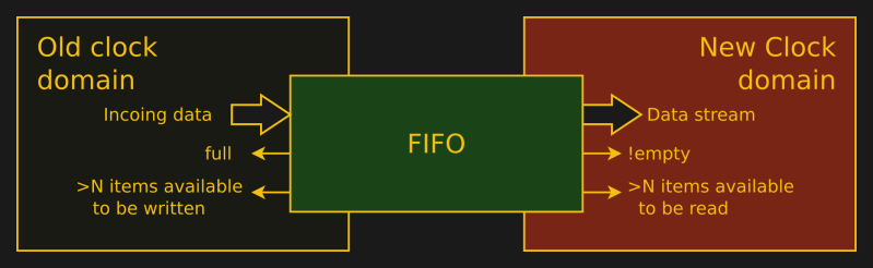
What’s “Incoing data”?
Something a Klingon engineer would deal with.
You couldn’t come up with a Worf pun?
The linked source artical seems more informative: http://www.sunburst-design.com/papers/CummingsSNUG2008Boston_CDC.pdf
That’s a great paper. Everything I’ve read from that guy seems excellent (to me as a novice)
It’s really good for a novice. Kinda wish, considering how detailed things are, that there was an appendix of caveats. Or even the *mention* that MTBF is *exponentially* related the amount of time you wait for the metastability to settle. If you’ve got a 10 MHz clock you can get away with a ton that you can’t get away from with a 400 MHz clock. And it’s not bad design to do so – it’s actually understanding what’s going on rather than sticking to rules-of-thumb.
There’s also fpga4fun’s articles on this:
http://www.fpga4fun.com/CrossClockDomain.html
The flag synchronizer in there is the one I use all the time in my designs.
All the video shows is that his FPGA is really good at avoiding metastability.
I have not seen an actual case of metastability in the whole video.
In most cases some extra jitter is procuced because of marginal timing.
In some cases the FPGA does not switch at all, because of timing violations.
He would have shown true metastability if ( AND ONLY IF !) there would have been a signal with a significantly deviation from the (about 2ns) rise time of a flank. I have not seen a single trace with a rise time of >3ns.
A real showoff on metastability would have been if I had seen a signal with a 10ns rise time or a signal which starts to change and then falls back to it’s original level.
The extra jitter is for a large part introduced because of driving his FPGA from a voltage source which is out of spec for his FPGA.
So this whole post is nonsense at best or misleading at worst.
Yuch.
Metastability in an FPGA shows up as effects from timing violations. You can’t see the actual metastability behavior because the signals are internal. All the external signals typically can’t show metastability because external signals are very slow compared to the internal ones.
But you can actually see the behavior if you’re really clever, like forcing a signal into the metastability window using the fine phase shifts on a PLL and sampling with another fine-phase shifted clock to probe things at literally picosecond scales.
Another good piece of document I would like to add is “toggle synchronizer”
https://inst.eecs.berkeley.edu/~cs150/sp10/Collections/Papers/ClockCrossing.pdf