
I recall the point I started taking electronics seriously, although excited, a sense of dread followed upon the thought of facing the two main obstacles faced by hobbyists and even professionals: Fabricating you own PCB’s and fiddling with the ever decreasing surface mount footprints. Any resistance to the latter proves futile, expensive, and frankly a bit silly in retrospect. Cheap SMD tools have made it extremely easy to store, place, and solder all things SMD.
Once you’ve restricted all your hobbyist designs/experiments to SMD, how do you go about producing the PCBs needed for prototyping? Personally, I dread the thought of etching my own boards. The process is laborious and involves messy chemicals and specially sensitized PCB’s — none of which interest me. I’ve only ever done it a few times, and have promised myself never to do it again. Professional but cheap PCB manufacturing is more like it board pooling services such as OSH park have made this both easy and affordable — if you can wait for the turnaround.
So what are the alternatives? If you are really serious about swift prototyping from your own Lab, I put forth the case of milling your own PCB’s. Read on as I take you through the typical workflow from design to prototype and convince you to put up with the relatively high start up cost of purchasing a PCB mill.
Tools of the Trade:
The Mill:
In recent years the frightening cost of buying a CNC machine both rigid and precise enough for the job has come down significantly. A quick search on eBay and Aliexpress for “Engraving CNC machine” returns some interesting and affordable hits. The generic machines floating around on these websites are called CNC 3020 denoting a work area of 30cm by 20cm and cost around the £250-£300 ($350-400 USD) mark. Other models are the 3040 and the 6040. The machines seem to all be based on a single design (and even a manufacturer) and are well built. The aluminium based construction is solid and handles an array of materials given the right spindle of course.
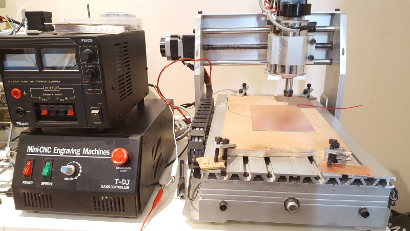
The cheapest machines tend to host a simple DC 50W electric spindle which is reliable enough and more importantly, cheap to replace. It is suitable for engraving and cutting woods at modest feedrates but nothing more. The more recent machines are coming with water cooled 200W spindles that are certainly a better choice. You can cut modestly thick aluminium with them too.
I had purchased one of the early versions of the CNC-3020 quite cheaply. The machine had no end stops, hosted an old parallel port based interface and had most of the PCB functionality such as auto spindle control unpopulated. We wrote an article awhile back where [whitequark] successfully modified his machine to upgrade the hardware. I too did the necessary modifications, which were simply attaching 3 end stops to the CNC and soldering in an otherwise unpopulated connector for the surface probe. Many of the newer machines sensibly come with these pre-installed now.
The Bits
With the machine ready, we need to get the right tools for milling PCBs. The most important of these is the engraving bit, responsible for committing all the actual traces onto the PCB. This bit needs to be sharp so it actually cuts as opposed to tear the copper and of course it also needs to be fine enough to mill any tiny footprints or traces. After a lot of experiments, I’ve got the best results using generic 0.1 mm V bits from eBay. These are cheap and reliable enough for about 8-10 medium sized jobs. However, the V profile does pose a challenge when specifying its cutting width in software, as the deeper you go the wider they cut. This can be tuned via some trial and error.
Next, we need a few drill bits for drilling through-hole component mounts and vias. Every different hole you specify will need a manual tool change, so its best to simply stick to a single 0.8 mm – 1 mm bit which should be suitable for most things. I would recommend buying this set of cheap drill bits.
The last bit we need is the End mill, responsible for cutting out our board from the larger PCB clad. A 1-2 mm End mill does the job nicely.
Apart from the above essentials we also need the actual PCB clad, I’ve found the generic, cheap, single sided ones on eBay are terrible, they crumble like biscuits when being cut. All the better ones seem to be double sided, in either case I had to experiment with a few different suppliers before settling with one I liked. Sourcing quality copper clad seems to be a topic that hasn’t been settled throughout Hackaday’s history.


Miscellaneous
In addition to the important items listed above, we will also need the following:
- Thin Double sided tape to fasten the PCB clad to a scrap cutting board for the CNC. This should not be the foam backed but rather the thin-film one often used for fabrics.
- A Finishing brush with stiff metal bristles for some post processing. A board fresh out of the CNC will inevitably need to be deburred.
- A fine sanding block or sanding paper to clear away some of the more finer burrs.
- Rubbing alcohol and a softer brush (I use a toothbrush!) for the finishing touches.
The Mechanical Setup
The biggest challenge in this DIY process is getting a correct and consistent cutting depth. These V-bits yield a wider cut the deeper you go, effectively robbing you of precious engraving resolution. If you do not tune in just the right depth, some traces will come out too thin and frail. The key to success is to experiment with a few cutting depths and most importantly probe the PCB to compensate for any variations in the height across the clad.
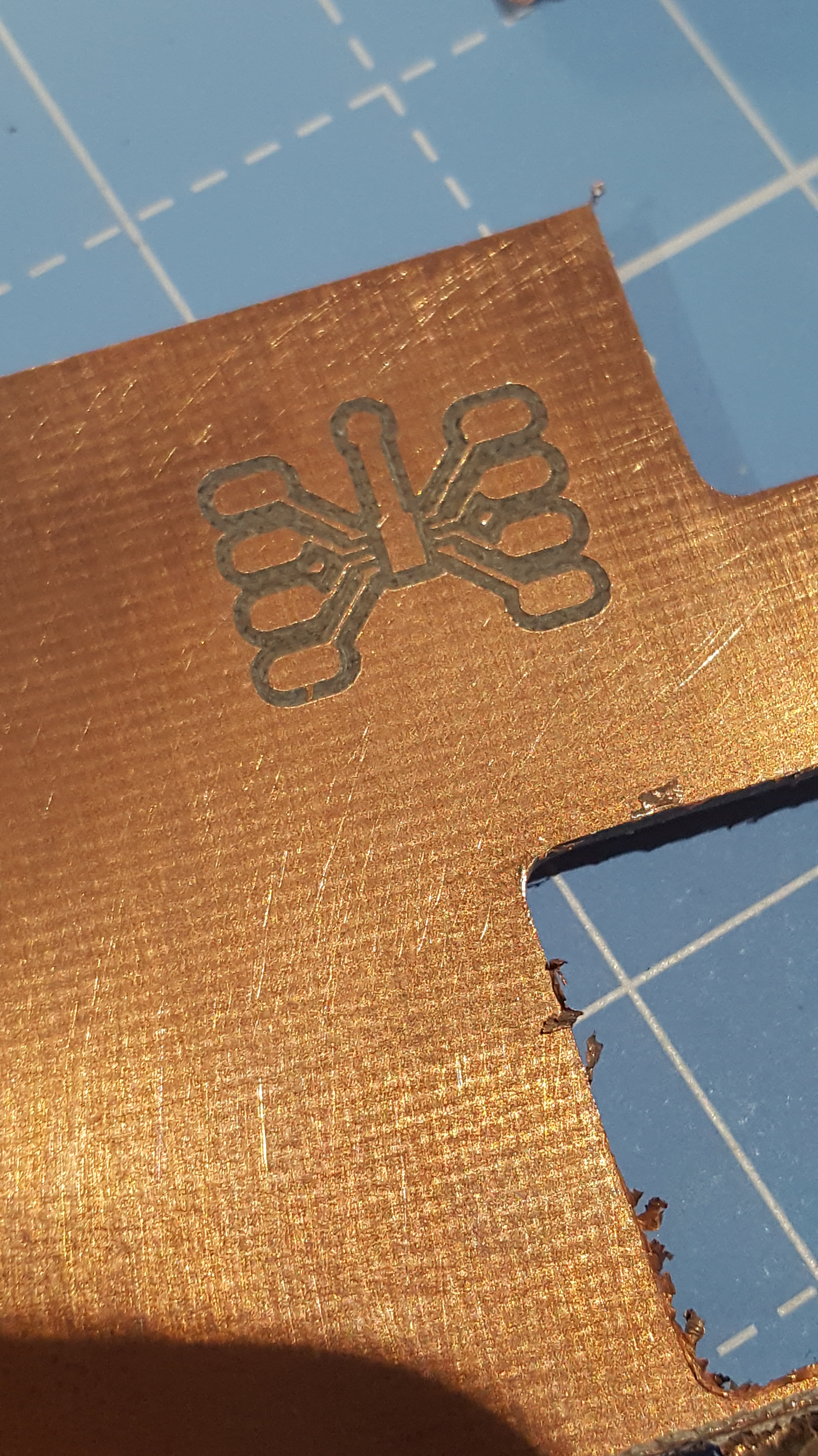
To tune the right cutting depth, I put together a simple test design consisting of breakout board for the super tiny DFN-8 footprint. The trace size on this board is as small as my designs would go. Next I tried a few different cutting depths and eventually found one with reliable results for these thin traces. I use a cutting depth of 0.8 mm with a 0.1 mm V-bit.
Preparing for Auto-Leveling
The auto-leveling process is set up in software and simply consists of a probing routine before milling. All we need to do is to solder a scrap wire to a corner of the PCB clad, and fasten it to an ideally flat piece of scrap wood using generous amounts of double sided tape.
Once this is complete, the wood is secured to the CNCs work area and the milling bit is secured in the chuck. A pair of crocodile clips are attached to the wire soldered on the PCB and the milling bit, completing the probing setup. The idea is to build a map of the height variation of the PCB, and if the PCB is not completely level, the mill will actively compensate for the error.


The Software
PCB CAD
The first step is to prepare the CAD files, all we need from our favourite PCB CAD software are 3 GERBER files: Top, Bottom and Drill. But before we do that, we need to make sure all necessary precautions have been taken to maximise the mill’s chances of reproducing the circuit
As an example, lets talk about some things I ensured when designing the following PCB that I have milled successfully quite a few times now. For anyone curious this is the Phase Lock Loop section for a DIY Spectrum Analyser based around the Analog Devices ADF4008 IC.
- Choose footprints wisely: This board is based around an IC available in both TSSOP-16 and LFCSP-20.
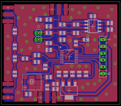
The Board: Phase Lock Loop with VCO Amplifer Milling for the later, tinier package would certainly be pushing the capabilities of the process. As a smaller footprint also imply smaller traces, this makes the whole process a lot less reliable. With the same rationale I stuck to 0805’s or 0603’s for passives where possible.
- Trace to Trace clearance: As a rule of thumb I kept trace clearances to at least twice the width of my bit. With a 0.1 mm bit, a minimum clearance of 0.2 mm is sufficient.
- Pour Clearance: One of benefits of this subtractive process is that you have natural ground plane at your disposal. However, finished boards tend to have copper burrs around traces which can short with a ground pour placed in close proximity. Hence, pour to trace clearance should be at least 0.3-0.4 mm. This will also make reflowing the board without a solder mask a lot easier.
- Trace Width: Once again, anything larger than twice the bit width should work nicely. I generally stuck to 0.3mm traces
These constraints are certainly very restrictive compared to any professional fabrication but with a bit of give and take you can certainly produce usable and realistic boards.
FlatCAM
Once we make sure all the above constraints are respected we need to export the GERBER files and then turn them into GCODE that the CNC could run. For that we use an excellent piece of open source software: FlatCAM, which is specifically designed for 2D PCB CAM processes. It has an extensive set of features that you should really check out.
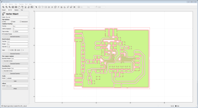
A tutorial on FlatCAM is beyond the scope of this article, for that check out the official documentation. In summary, for each GERBER file you import, you have the option to generate various tool paths for different kinds of jobs such as Cutout, Isolation milling etc. All you need to do is punch in some parameters specifying your cutting depth and bit sizes.
For a single sided board, we need 3 GCODE files from FlatCAM; Top-layer, Drill and Cut-out. With those in hands we are almost ready to mill out our board!
Auto-leveling
The last software step is to add an auto-leveling routine by post processing the Top-layer GCODE file FlatCAM produced. For this we use yet another excellent piece of software called Autoleveller, which we featured way back.
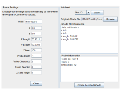 There is a free version and a paid version, the free version lacks the ability of sharing probing data across sub-jobs. This is somewhat important as you can only probe the board once at the start of a job, i.e you cannot probe for the drilling job after you have already cutout and hence isolated part of the board from the PCB clad! Honestly, I haven’t felt the need to purchase the full version yet, as probing is only critical for milling traces.
The most important parameter of this process is the Probe Spacing which determines the probing resolution. The smaller the Probe Spacing, the more points probed. Although this takes a while to do, it is well worth doing at least 80-100 for good results. Once this file has been generated, it replaces our old Top-layer Gcode file and we are ready to mill out our board!
Milling It Out
At this point we will have 3 files for our single layer board: The top layer file with probing, the drill file and finally the outline milling file. We begin by milling the top layer file. Fire up your favourite GCODE interpreter/CNC controller, I use MACH-3 but Linux CNC or most others are all viable options.
We begin by homing all 3 Axes, positioning the spindle roughly a few millimetres above a corner of the PCB and zeroing all 3 axes. It is important not to lose track of the X-Y zero position between the different jobs. Each new job will need a re-zeroing in the Z axis but the X and Y zero positions will be unchanged. Make sure the probing circuit is correctly set up, otherwise the mill will crash into the PCB! Once we engage the job the Mill should start the probing routine. Once complete, the milling routine will begin, depending on your feedrate and number of passes, this usually takes a while. Once this is complete our board should hopefully resemble our design albeit cluttered in fibreglass dust.
Next, we move on to the drilling, this step does not need precise re-leveling. We simply insert the drill bit, and zero the Z axis with the bit laying flush against the PCB surface. Once this is complete all the specified holes should be drilled into the board.
Last but not least, the board needs to be cut out from the rest of the PCB clad. This process is very similar to the previous step albeit with a different bit and slower feedrate. Once again we re-zero the Z axis and let the job run. If all went well we should have the finished PCB!


Finishing Touches and Assembly
Now onto the more rewarding parts of the process. The milling process is not perfect, especially as the engraving bit gets blunt, it tends to tear rather than cut. To clear off stray copper filings, give the PCB a good scrub, first with the thick bristle brush and followed by the finer sanding paper. After a final wipe with some rubbing alcohol, we can finally solder the components on!


Take a look at the final result. It looks pretty good, although you can see some imperfections such as residual copper traces in between actual traces. These should not be a problem as we specified sufficient clearances between traces and pours!
What next
Now you might be wondering if this process works for double sided boards? The answer is Yes. Although aligning the two sides can be a bit of a hassle, with the right practice and jigs this is not too hard.
In fact, FlatCAM provides a way to drill alignment holes for aligning 2 layer designs. Lastly, you might also be wondering if this elaborate workflow produces consistent results for demanding footprints. The answer is again, Yes. I have produced multiple boards for packages as small as DFN-8 (3 mm * 3 mm * 8 pins!) in a single run! Check out this 1 GHz mixer based off the LTC5560 IC in DFN-8.


What does SMD have to do with it? One could certainly use this same method to create a board for through-hole components!
I kind of see people telling me I should be using SMD as similar to people telling me that I should be using Metric. They have a lot of great points and in a perfect world would be right but they are completely discounting that someone else’s personal situation might be different from their own.
In my case that would be a garage full of boxes of through-hole components and local hardware stores that carry just about every fastener, cutting and measuring tool I could ask for in Imperial but only a tiny selection of over-priced metric items if they have any at all.
It’s not like that really adds anything to this particular conversation. It’s annoying, cut it out!
The board I manufactured here is an RF Mixer for >1GHz. Try and do that with THT. As much as I enjoy the ease of THT, confining yourself, as a matter of principle keeps you from doing a lot of things eg RF.
IMO smd is much easier than THT, no constantly flipping the board
Provided all your components are on one side…
Not just for that, insert component, flip board, solder it, cut wires, flip it again and repeat. SMD are far far easier. Just place and solder, no cutting wires and flipping board. Doubleside board does not matter, every side at once.
Flip – solder bottom side components – flip – solder top side components.
Two flips.
I only flip my board twice. I pull all through hole components onto the board for one side, bending the axial wire as i stick them in so they secure themselves. Flip the board solder all components, trim the legs and done. But I also do SMD for high density boards.
Ask, and you shall receive:
https://www.minicircuits.com/pdfs/SBL-11+.pdf
Really, the main things you can’t do in RF with through-hole components are amps: everything else it’s not that big a deal since they’re already fairly lossy intrinsically. Just more expensive.
LOL. So people responded with reasons to use surface mount. i’ll repeat.
“They have a lot of great points and in a perfect world would be right but they are completely discounting that someone else’s personal situation might be different from their own. ”
So… I won’t try to do >1GHz through-hole construction. So what? that doesn’t make me want to throw away boxes of through hole components and buy all new in SMD. Well.. not unless I some day find that EVERYTHING I build is > 1GHz. I don’t think that is going to happen though and meanwhile I see no reason to be that wasteful.
More central to my point though.. I can CNC a board for either one, surface or through hole mount. So.. why does an article about etching boards on a CNC even have to open up that pointless debate?
why U so mad?
Probably because you can breadboard through hole components but not SMD (without breakout boards), so the main impediment to using components that are only available in SMD packages is the inability to quickly put together a prototype circuit. So… here’s how to get around that without having to deal with nasty chemicals*.
*aside from the carcinogenic-if-inhaled airborne dust
If we compare the workflow, people plugging through-hole components into solderless breadboards are not likely to be at all impressed by the claimed convenience of having to design and manufacture a proto PCB to replace the step of “take breadboard out of box, grab a handful of jumpers and drop them on the desk.”
If you know for sure that the circuit you’re designing will be a product, then starting from SMD has benefits, especially if you’re doing another standard implementation and don’t need to build a proof of concept first. But I think most people building their own circuits aren’t in that situation; maybe it will become a product eventually, but probably it won’t.
The complaint isn’t that there are people using SMD, the complaint is that many of these people then turn to those using THT and tell us we’re doing it wrong. We’re not.
The SMD nonsense is just that; nonsense parading as information. Which I like best is my opinion; which you like best is not my opinion, just nonsense.
The actual topic of the story though is not about SMD vs THT, it is about using a mill to manufacture a PCB. For people using THT it is just as useful as people doing SMD; after all, they do make SMD proto boards, the SMD people didn’t really need to design a PCB to make that jump.
The only This vs That that should be in the story is Milling vs Etching vs Ordering.
* I use emacs for programming and vim for system administration, that’s why I’m an expert.
If you are doing through hole with double sided clad board you are milling both sides. As the article points out, its doable, but raises the pain and complexity quite a bit. Thus SMD is far easier, and you get to use the other side for an RF ground plane. :)
If you use single side copper clad, it’s quite easy to do through hole. But you can’t get the SMD density.
In my garage, the boxes full of through hole are mostly gone as almost all manufacturing has gone to SMD. Sure, there are a few things that still use/need through hole, but it’s vanishingly small. You used to be able to pick up lots of surplus through hole @ hamfests, but it’s mostly SMD partial reels at this point.
Not to mention a complete E24 resistor/capacitor assortment fits in a box that’s 20cmx30cmx2cm.
“you are milling both sides. As the article points out, its doable, but raises the pain and complexity quite a bit.”
So.. i guess you create double sided boards but with no vias so each side is like it’s own isolated single-layer PCB? Once you add vias you need good top/bottom alignment no different than with a through-hole board.
As for ground planes.. even if every project I ever worked on involved RF I could still use my old through-hole supplies to build power supplies, control boards and whatever else does not need the groundplane.
SMD density only really matters if I am trying to compete with portable, commercial products on size and weight. My stuff is far more likely to be one-offs that live in my house or maybe in my car.
“You used to be able to pick up lots of surplus through hole @ hamfests, but it’s mostly SMD partial reels at this point.”
Wow. We definitely are not attending the same hamfests! In my area they are still mostly through-hole stuff. That’s how I ended up with a garage full of it in the first place!
“In my garage, the boxes full of through hole are mostly gone as almost all manufacturing has gone to SMD”
My garage is more of a hobbyist playground and not a part of the manufacturing industry.
“Not to mention a complete E24 resistor/capacitor assortment fits in a box that’s 20cmx30cmx2cm.”
Good point. But… it’s all the salvaged mechanical pieces that really clutter my workshop. While my components may take more space than yours eliminating them wouldn’t really make a dent.
Good point. I have a corner devoted to components, the rest of the mess is dead devices (mostly year sale finds that are salvaged)
Seems like there’s some very good arguments for SMD in RF applications. Kind of like how there’s some very good arguments for metric. Maybe the complaining comments are really what detracts from useful and constructive conversation?
Most hobbyists need to be able to use both metric and standard units. So anybody telling you that one is wrong is tilting at windmills.
And then somebody else says, “Gosh, I don’t like complaints, how dare you complain about people complaining!” And it seems to me to not be self-consistent; the original complaint isn’t complaining about the existence of complaints, it is complaining about the existence of other people’s choices, and then the response is to complain that the specific complaint made (“this should be in metric”) is out of place and pushy. And then the third person says “maybe the complaining comments are really what detracts,” and they don’t even realize that they’ve addressed neither of the things the other people were complaining about, are talking about a different subject, and didn’t make any substantive point at all.
Maybe you’re right, but maybe you’re not, so maybe you should flesh out your ideas and check them for consistency?
Island routers are slow (like 3 to 5 hours a side on the unit we purchased), but these are useful for some types of problems.
Like super thick high-power switching boards, or tuned RF lines for example.
However, without through-hole plated via, this doesn’t really offer anything beyond classic chemical etching processes.
There was a time when a CNC process was used for deburring RF lines, but most high-speed mills generally seem to add more chowder than they can remove.
I’d recommend Chilipeppr or bCNC over Autoleveler. Both can do auto-leveling just as well but are free and nicely integrated.
+1
And look at the woodpecker CNC controller.
If your on windows, openCNCpilot is a nice simple gcode sender for grbl with autolevel. No web interface like chilipeppr. bcnc is pretty nice.
I was using mach3 but loosing steps due to an issue with an add on parallel port card, An arduino running grbl to the parallel port input on the 3020 cnc runs much smoother and more reliable, it lets me use usb. I was using the same tool chain that the author write about, eagle –> pcb-gcode –> autolevel –>mach3 –> cnc. Grbl has a different probing approach so the tool chain is now eagle –> pcb2gcode –> openCNCpilot (w/built in autolevel) –> Grbl –>CNC
Woohoo! I’m a big fan of using these cheap CNC mills for PCBs!
Buy used 1/32″ endmills from eBay https://www.ebay.com/itm/Ten-Pieces-2-Flute-Carbide-End-Mill-Bit-1-32-Made-in-USA-pcb-cnc-Dremel/151100157888
They’re so cheap you won’t even sweat throwing them away when they go dull.
I think by using endmills you don’t need to do any auto leveling. And you can use the same tool for trace cutout, board outline, AND DRILLING.
Make sure you’re buying the FR-1/Bakelite boards and not fiberglass. I just get them directly from Bantam https://www.bantamtools.com/collections/materials/products/pcb
I use 2″ wide double-sided crepe paper tape for my hold down http://amzn.to/2CTMIyd . I feel it’s easier to get it flat than the plastic double sided tape.
We’ve been using CNCJS driving a GRBL arduino connected to the mill https://github.com/cncjs/cncjs
I hope more people start doing this. It’s super fun!
good tips, thanks
I have had great success with these https://www.ebay.com/itm/NIAGARA-Carbide-End-Mills-017-4FL-0255-LOC-x-1-1-2-59925-Qty-2-1080E170/122586415379?ssPageName=STRK%3AMEBIDX%3AIT&_trksid=p2057872.m2749.l2649 .5mm endmills that come in a two pack for super cheap
Agreed. I use an endmill for the engraving and to drill holes. I do things in the opposite from the author. I drill first, then engrave.
But even with an endmill the results I get from leveling with a probe using AutoLeveler are much nicer than the “dig in” that I get with just finding the high part and over-engraving one area to make sure another area is properly engraved. I have done some re-runs on my boards to compensate for uneven copper clad.
Drill first. Nice tip, thanks!
Is there any advantage of drilling first?
I do the milling first. My hint for drilling: 0.8mm drills tend to wander around (and when carbide then break ;) ) sometimes, but a broken-off carbide drillbit that has 2-3mm left works remarkably well and doesn’t wander anymore, making very clean holes. (some of my milling can be seen in the YT links from here: hackaday.io/project/24926-arduino-driven-led-display-with-bt-data-transfer)
greetings
Is the hobbyist market that big, or is this more small shops, and one-offs?
If your market is big, the time this takes is prohibitive. This is just for the prototypes in that case, and you’d send away for the production boards.
Agreed. Doing it using the milling route can take a while to get set up and perfected. But afterwards the turn around time is hours instead of weeks via the mail. For prototypes it’s a great solution. for production not so much
Unfortunately the CNC 3020 links (not the hackaday article link, the included links in that articel) are down…
AliExpress/eBay are full of these 3020 (or larger/smaller – the numbers are dimensions) machines. Just search for “CNC 3020”.
The problem with it is that the machine usually comes with a crappy spindle with a large runout and shaft that will flex under load -> poor result. Look for a variant where the spindle is belt driven and sitting in a proper bearing.
Many of these will also need some non-trivial hacking to make them work with modern computers that don’t have classic parallel ports (the electronics is just a few power transistors controlled over parallel port, with all the negatives that brings).
The probing circuit required for leveling is also something you will have to build extra (not difficult), as will be a sacrificial board and something to actually clamp the workpiece down. The clamps some of the vendors ship with it are universally unusable.
So you buy a $800 machine but expect a lot of modding before it will be actually usable for this kind of job.
I personally don’t see much point in milling these types of boards – it takes a lot of preparation, the milling itself is a slow, noisy (not good if living in a flat!) and very dusty (you will need something to vacuum the dust out and don’t mill FR4 -> dust is carcinogenic!) affair.
By the time the board is finished by milling I would have the same thing likely done and populated already if I do it by regular toner transfer or photolithography – and in the latter case with better resolution than what is achievable by these cheap mills too. The only issue is drilling holes for through-hole parts but a decent drill stand is much cheaper than a CNC mill and the few holes a typical surface mount board has are done in no time.
Milling has its place where precise surface dimensions are needed, like some microwave designs. But for general prototyping? Why?? Some people are scared of the chemistry but I certainly prefer dealing with something like a ferric chloride than the noise and dust from a mill, especially in an apartment.
Oh and don’t forget that one can get ten 100x100mm boards for $2 delivered *** in a week today – with two layers, solder mask, plated-through vias, silkscreen and routed to any shape you want. Why would I bother with something like milling then? I make my own boards only for various adapters/breakouts I need right now, otherwise there is no point.
*** That’s a special price from JLPCB, but even their normal ~$20 is pretty good, especially given the rapid turnaround time.
See my comment below, $230 all in including the Pi (which connects to the mill with USB) and the limit switches.
Milling is good when you are doing small SMDs with fine pitch. I always seem to manage to etch the traces away on them waiting for other places to finish.
I concur that send it out is the way to go for multiples. But these are great for prototyping. Prove out the design, avoid latency reving the boards from Asia. Yes, they are noisy, but, like you, I can get a small board out, including drilling in under 20 minutes. And I don’t have to explain the chemical small and disposal issues to the spouse. Different tools to do the same job. To each their own.
I found this inspiring, although I wouldn’t use such a setup for PCB’s. I’m thinking about keyboard keycaps.
A small frame could hold a few keycaps flat, or on their side (to allow engraving on the front). Depending on bit size and shape, you can even have variable width in font strokes by deliberately varying drill depth. Fill in the groove with paint and/or resin, for a long lasting finish.
I picked up a similar mill @ MicroCenter for about $200US. Has a Woodpecker GRBL based controller. No end stop switches, but that took a couple of hours end to end.
http://www.microcenter.com/product/473125/mini_cnc_engraver_machine
I added a Pi Zero W to it and it is totally stand alone with chillipeper. You can even drag and drop Eagle files right on it and it spits out boards.
Great tutorial. I use the Bantam CNC (formerly Othermill) for this, which is what it was designed for, and that makes the software side much easier. But given that PCBs can be fabbed by companies like OSHPark in a few days for as little as a dollar, I don’t do much milling anymore. Why not just use OSHPark and with a few clicks get two-sided boards with vias, which are really hard to do with a mill?
> But given that PCBs can be fabbed by companies like OSHPark in a few days for as little as a dollar, I don’t do much milling anymore.
I’ve never understood why people quote OSHPark prices as being so low, they aren’t. They’re $5 per square inch for a 2 layer board, plus shipping. And usually shipping is the main cost… JLCPCB is the cheapest price I know of at $2 for 10cm x 10cm, but shipping is not free and costs around $10 on top.
OSHpark is $5 per sq inch for a 2 layer board, but you get three of them. So effective cost is $1.66 per sq inch. Shipping from OSHpark is free using regular postal mail. Yes if you want to expedite the fab and pay for faster express shipping you can do that, but it is not required.
More recently I’ve been using dirtypcbs.com where you can get up to 10cm x 10cm, ~10 copies, of a standard 2 layer PCB for just $17 plus $9 shipping Hong Kong airmail. Couple of weeks in my experience. Four or more layer boards are not that much more expensive (compared to OSHpark). So $26 for ten boards that are about 4 sq in each
> Shipping from OSHpark is free using regular postal mail.
Only if you live in the US, which (and especially those living in the US tend to forget) most people on earth do not.
dirtypcbs is a horrible service; low quality boards and slow shipping. But even if you go for a good service with reasonable fast shipping (which’ll only take a few days around the globe) it wouldn’t break the bank…
OSHpark is okay and for those living in the US certainly one of the best local and for that rather cheaper options. In Europe for example there’re really not that many good *and* affordable PCB manufacturers, though there certainly are very good expensive ones.
Just to correct this point here: We (OSHPark) have had free international postal mail shipping for the better part of 4 years.
Hey Laen, I’m glad to hear that.
And just to say it again, OSH Park has saved me countless hours of frustration – when I send you my KiCad-produced Gerber files, I get back exactly what I expect, and for me it’s well worth the wait. And I actually LIKE the purple solder mask. Nobody but us hobbyists even know what it means when they see a purple board – everybody else just says, “ooh, pretty”.
Is there a ulp or another easy option to make gcode to burn the paint away starting from gerber files? most of the stuff i have found is for isolation routing..
The Gerber format was developed to drive a Gerber photoplotter, which is basically a 2D CNC machine, so it’s basically already a list of X-Y moves. I would think that it would be a pretty simple thing to translate each line in a Gerber file to one or a few lines of G-code. It does use ‘apertures’ for pads so it doesn’t have to specify the path for each individual pad, but again, each aperture would translate to a number of discrete moves. But no, I don’t have the name of any software that does this. I think the easier and maybe faster way is to generate raster files (.png format), which there are several programs that can do (I use gerbv for final verification, and it does this), and etch it as a picture.
Since you are talking ulp, I assume that you are using Eagle. I just get Eagle to export a Bitmap (BMP) at the resolution of my laser cutter (500 x 500 dpi – Full Spectrum Laser), and then just use the Laser program to raster the bitmap. Traces are not as good as they would be from milling or from photoresist though. Good enough for 15mil traces and spacing, but don’t try to do this with 0.5mm pitch SMDs — at least I haven’t been successful with it. If anyone out there has more success, please comment and let us know.
Because of having to wait for three, four or more weeks for the boards to arrive kills the mood and break the concentration of the development cycle.. Shipping from OSHPark is not that fast to all places in the world ( and also not that cheap )
+1 I like OSH Park, Seeed (for white mask, no code) and other suppliers too for beautiful boards, and I like milling for when I want to finish the project today.
$300 buys a lot of express shipping…
As most of chinese express shpping rates fall around the US$ 50 mark, it would be good for just a couple.
I’ve tried this as well as just laser engraving the pcb but by far the easiest way I’ve found is to spray paint the bare copper, use the laser to burn just the paint off of where it needs to be etched, then use muriatic acid mixed with hydrogen perroxide (I’ll have to go look at my notes for the mix ratio) then after etching wipe down with MEK to clean the remaining paint off. Using a router works ok, but I’ve found the cheaper machines to be tedious and setup takes longer than just etching it with a laser and acid.
going to try laser method at home so:
what power laser do you use?
what is your min trace width?
does type of spray paint matter?
I’m interested in this as well. This sounds like the easiest way of all. I don’t have a laser cutter, but if it doesn’t require too much power (like more than 5 watts), I could put a laser module on my CNC engraver, which would make it AWESOME. All of these other methods have SO many ways to screw them up.
Lots of pollution with the chemicals…how do you live with that?
In my mind it all gets down to the density and size of the traces or the overall complexity of the board. I can see milling simple boards, but I don’t think milling a complex board would work well. I also agree that you doing double sided boards would be harder with a mill. There is a reason that photo etching has been around for so long.
I don’t see how registering the second side in a mill would be any more difficult than doing so with photo etching. That’s really the least of the difficulties.
Do the vias in this design serve a purpose?
I would have figured they were fencing vias, but they haven’t been connected to the (assumed) bottom ground plane.
It is possible that these are, indeed, fencing vias and are left in for when plated vias are an option, foregoing them in the milled version seen here.
Anyone could make a calculation on the cost of doing a 100mm x 100mm board, with all consummables involved (engraver bit) — just to compare against outsourcing? I saw the 20 minute figure , just all for comparison using this versus costs of ethching too.
I dont see any monetary advantage other than being able to iterate much quicker.
If you have the time, source it out, if you want to be fast, do it yourself :)
I recently converted my old Ordbot Hadron 3D-Printer to a PCB-mill and was not that excited about the finest pin pitch I could manufacture. Now im going to make a hybrid process with drilling and milling first, then Toner-Transfer and etching after. We will see how that works.
For actual PCB’s I usually order them from OSH Park. For when I need something quick and dirty, I often use perfoard. And because less than 10 cents per 5×7 piece of perfboard isn’t cheap enough for me, I often break out eh Dremel and cut off the unused portions for later use.
“less than 10 cents per 5×7 piece of perfboard” … unless you need spacing < 2.54mm, at which point it becomes either very expensive (cheapest price I've found for 1.27mm perfboard is $10 for a tiny sheet) or completely impossible. I've never found a perfboard that would work for 0.8mm spacing required for TSOP components (which you need for most large capacity RAM chips) or 0.5mm for QFP (which you need for most modern programmable logic devices, e.g. CPLDs or FPGAs). You *could* try using breakout boards for those, but with signals in the hundreds of megahertz or lower gigahertz range it might not work very well.
I tried FlatCAM, had difficulty getting to run under OSX. Played around a bunch with Carbide3D’s web tool and was very impressed with the quality. Other than an unexpected “zero offsets” in the produced GCode, worked perfectly. http://carbide3d.com/apps/pcb/
I tried FlatCAM, had difficulty getting to run under OSX. Played around a bunch with Carbide3D’s web tool and was very impressed with the quality. Other than an unexpected “zero offsets” in the produced GCode, worked perfectly. http://carbide3d.com/apps/pcb/
nice to see a write-up on the technique. i started with doing the whole design/print/etch method, but got tired of all the steps and the personal inconsistencies i have with etching.
these days, if i need to make something, i do the layout, print it out on normal paper, and then tape it to some copper clad, using a dremel with a cutoff wheel to cut the traces. it’s not pretty, but it works. the smallest component i’ve needed is SOT23-6, so not small enough that i need any more detail to the traces.
I’ve stayed away from milling for hobby PCB needs because it becomes a whole hobby in its own. They’re getting better though as demonstrated above. It is hacking so you can do electronics hacking.
I’ve stayed away from photoresist for hobby PCB needs because it becomes a whole hobby in it’s own, and progress seems to have stagnated. It is hacking so you can do electronics hacking.
Bought one inkjet printer just for PCB use, pretty sure it was HAD saw it on long time back, special etch resist cartridges, worked somewhat, needed improvement but worked. Was almost there… just shy of making the grade.
We’ve been stalled for years at this level, but the bits of progress here and there such as this example are interesting.
Am still using laser printer transfer, and for quickie small stuff the sharpie by hand. Still have some datak rub-ons that work ok, they’re etch resist themselves, but getting old.
Perhaps can drag together a couple junk laser printers and build a double-sided laser scanner to expose pre-coated photoresist boards directly…. but again, another whole hobby to develop on it’s own.
30 yrs ago believed we were on the edge of some new great hobby toy that would solve this for us. Many like this one been ok, kinda, but hey folks… we’re stuck in sand and spinning wheels all this time. Somebody is gonna get rich when they come up with one, but time is running out, things are getting so tiny.
One desperately needed part of the hobby is 20+ yrs behind here. Nothing has been “up to it” yet. Almost, but no bell ringer.
Until someone creates a home chip tech fab… just like Jeri Ellsworth were trying to do.. https://hackaday.com/2012/07/09/make-your-own-integrated-circuits-at-home/ rinse/repeat hehehe wish thris could come to fruition soon
“Until someone creates a home chip tech fab” — Until? https://www.deepdyve.com/lp/wiley/a-portable-benchtop-photolithography-system-based-on-a-solid-state-YZi3zHSwkp describes a fabrication system that can be used to produce 200nm scale semiconductors on 4″ wafers using a benchtop device that can be manufactured for less than $400.
Julian: I didn’t go past the paywall, but the $400 seems to cover only the UV illuminator needed to expose the photoresist. This is just the simplest of many devices needed to actually produce chips. You need to be able to produce the masks, which need to be reduced to actual chip size, with the patterns for each layer duplicated at precise intervals, you need something to align the masks so the various layers will be in perfect registration (within a few tens of nanometers), you need to be able to spin-coat the wafer with photoresist, you need a furnace to diffuse dopants into the lattice, you need something to score the wafer and then break it into chips, and you need a way to bond wires to the pads on the chips and then to either a leadframe or a PCB. And that’s just the things I know off the top of my head from being loosely connected with the fab process (I did laser trim and test development, so the wafers were already processed when I got them) about fifteen years ago.
Jeri Ellesworth demonstrated by making a huge MOSFET that the actual wafer processing steps were within reach for hobbyists, but this was on the level of making the masks from adhesive tape, not the level of producing chips for use.
Again, this could become a hobby on its own, and it would be great for that to become as available as CNC machining and 3D printing to a hobby community, but I don’t think the whole process is there yet. Somebody please prove me wrong.
And now that I read what I wrote, that’s really not many devices. Of those, the wafer scoring step could probably be done by a hobby grade CNC engraver. And somebody out there can probably figure out how to do lead boding; this is within the precision of hobby CNC equipment as well. Mask alignment? Don’t know about that one. I know that with a combination of mechanical steppers and galvos and a computer vision system (video microscope and pattern recognition software) you can get down into the 1 micron range, but even this is not for the faint of heart.
Hi Biomed, I agree with you 102% on this – It’s fun trying things that aren’t designed to work, like using an engraver to make PCBs, just like it was fun trying to get a laser printer to make a resist layer, and just like it was fun trying to use a pen plotter to draw the circuit using fine-point Sharpie pens. And even trying to use the “pro” approach of making photo masks, sensitizing the board, exposing and developing it, and so on, has a good size learning curve. But none of these things are fun any more when I’m trying to do something else, like get a circuit built. I have the opposite of ADHD; I HATE having to change tasks on the fly, because by the time I get back to the original task, I’ve lost whatever train of thought was going on there.
The method Cody describes above, using paint stripped off with a laser cutter sounds like maybe the easiest to get right – the etching part I’ve never had much trouble with; it’s always been how to get the resist pattern on copper that has been the problem.
I consider myself lucky that KiCad has reached a development level on par with the professional systems I’ve used in the past, and that there are now services like Seeed Studio, DirtyPCB, and OSH Park, so I don’t HAVE to mess with a bundle of kludges that I haven’t developed into a reliable process. My last three projects that needed PCBs, I went to OSH Park for, and in all cases I got back exactly what I designed. That is, any problems I had were design problems, not PCB fab problems. It took almost two weeks to get boards, but that’s two weeks I spent doing other things rather than two weeks and a lot of materials wasted trying to get a process to work.
Great writeup, thanks for that. I have some small issues:
\cite{ I use a cutting depth of 0.8 mm with a 0.1 mm V-bit. } – Is that a typo or do you really cut in almost a millimeter? This is way to much. Depending on the bit, 0.1-0.2mm (I use 45° carving bits) are more than enough to reliably cut through the copper (also depending on the rigidity of the Z-axis).
The cut-out board on your picture looke terrible – was the cutter blunt? I get clean cutting edges when cutting out FR4 board with a simple 2- or 4-flute cutter bit.
Spindle running at 24,000 RPM and I get very clean cuts.
A number of the Chinese fabs are supplying 10 copies of 100mm x 100mm or less boards for 5 bucks in green soldermask. 2 layer, silkscreen and soldermask on both sides. Add about $17 for DHL Shenzhen shipping and I reliably have my boards in 7 or 8 vslender days from when I ordered. That’s about $2.20 per board in your hands.
For the “but I could never use thst many boards” school who somehow feels ripped off because they *have to* buy 10 boards even if the out-off-pocket cost is lower than buying fewer boards from another source, you can also order 5 boards for the same 5 buck price. Huh, how is that a savings? You saving on shipoing costs.
I have printed Cyclone PCB Factory and am pretty close to milling my first board. However, I am having trouble centering the collet on the spindle axle. It seems to be identical to yours, two hex nuts. It is very sensitive to adjust, I always end up with the bit wobbling. A bad video here: https://www.youtube.com/watch?v=XHjIsq4VoC0 .
Any tips?
These spindles are notorious for being off centre. Mine was ok at the start but as the bearing/bushes wear out its getting worse. It seems your spindle is faulty.
I’ve done both: cnc milling pcb and chemical etching. I don’t understand why people claim that you have to deal with “nasty chemicals”?! Ferric chloride is pretty safe, it’s even used in water treatment. Not a big deal if it gets into the environment. It does stain your clothes and a lot of other things, but I used it when I was a kid in a chemistry set. Even the photoresist developers are pretty safe, sodium hydroxide is draino. Sodium carbonate is heated baking soda (yes, it’s found in your food). Stop thinking that they are “nasty” and give it a try. Both methods have advantages and disadvantages. I use cnc milling pubs when I need holes drilled for vias or a lot of through holes, photoresist if I need really fine pitch. Oh, and to answer someone’s question, you drill first before milling because you want to prevent the drill bit from walking.
I read that milling PCBs can cause lung cancer because if the tiny particals released in the air. Any of you taking that into account?
Where did you read that???
https://en.wikipedia.org/wiki/Silicosis
Hmmm, where did you read that – any details? how about allergic dermatitis first? If you are worried about the dust, try wet milling?
Drilling or grinding (or milling) glass fibers is the hazard here. One solution is to use paper/phenolic boards (FR-1 or FR-2).
Those should be quite sufficient for hobby projects anyway. I found in the end you can’t beat quality of even the cheapest board manufacturers. isolation routing is good for testing and prototyping, to confirm the design is alright. But in the end it leaves you wanting.
Bart, Yep,……. some kind of vacuum/filter system that sucks in the particles during milling will be very good — not only for the health, but less ‘sawdust’ to manually vacuum up after the cutting process. I am a fan of pcb milling though. This particular technique certainly is workable – provided the user has a suitable system (software, hardware, measurement/alignment/adjustment/setup methods). For the home environment, it can certainly be a lot better than dealing with chemicals. But….in any case….. whatever works for each of us…. is fine. And, as usual – safety is important…. so it is a good idea to wear masks and eye protection, and think about how the system can be set up to avoid health issues.
You don’t have to sand your board if you have sharper tools and proper settings, don’t settle for the shitty high speed steel ones, go for the cemented carbide. They do not wear out unless you plan on cutting hundred’s of boards, they can also do higher feed rates without heating up and breaking. Heat is your worst enemy for keeping tools sharp while machining.
Now with the right tool in place, use really high rpm, 30000 or higher is optimal.
Then keep your feed-rate at 50-100 mm/min.
Keep your depth at around -0.2 to 0.3 mm, if you go to deep you get wide tracks, to shallow and you get burs.
Drench your board in oil. This has to uses: Firstly, it keeps you tool tip cool so it stays sharp and hence you avoid burs.
Secondly, it catches all the dust so you don’t need to use a vacuum cleaner or you lungs to suck it up, just wipe it of when it’s finished. As a added bonus it also keeps the noice down as it dampens the vibrations.
It took me a couple of hours of thinking and testing to come to this conclusion but it was worth it. There’s a cheap 200$ CNC to the right of my keyboard running a PCB as I type this. I don’t even have to watch it while it’s running, just playing games and reading meanwhile. Never again will I use acids for making PCB:s, that’s just painfully time consuming and boring.