Maybe you are familiar with the op-amp as an extremely versatile component, and you know how to quickly construct a huge variety of circuits with one. Maybe you even have a favorite op-amp or two for different applications, covering many possible niches. Standard circuits such as an inverting amplifier are your bread and butter, and the formula gain=-Rf/Ri is tattooed on your forearm.
But you can know how to use op-amps without really knowing how they work. Have you ever peered under the hood of an op-amp to find out what’s going on in there? Would you like to? Let’s take a simple device and examine it, piece by piece.
The First IC Op-amp
The Fairchild μA702 was the first integrated circuit op-amp, a then-revolutionary component designed by Bob Widlar and first brought to market in 1964. Though it was long-ago deleted from semiconductor catalogues it has the advantage of an extremely simple internal circuit, one that can be easily explained in an article such as this one.
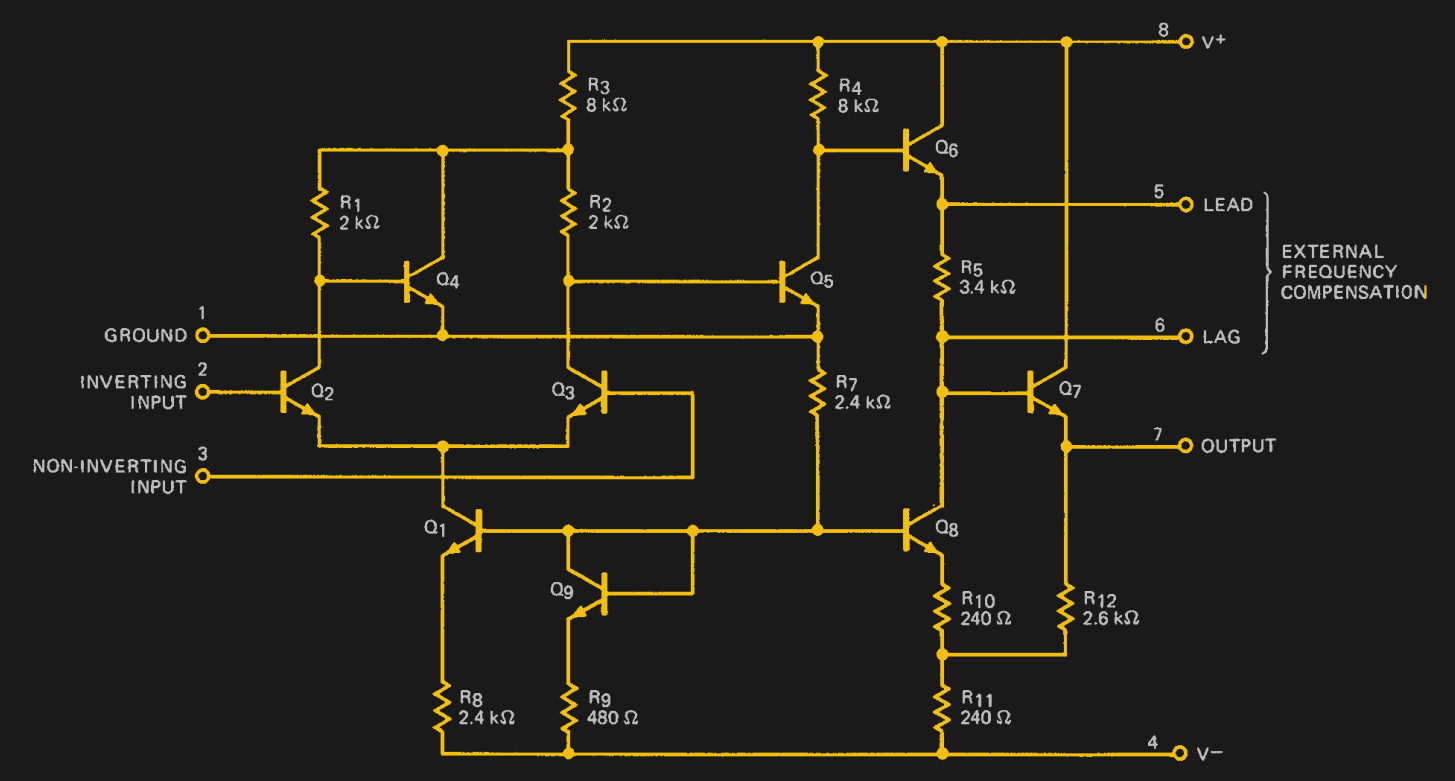
Even with only nine transistors, the μA702 circuit is not quite the simplest possible op-amp circuit, as it contains a few of Bob Widlar’s tricks to improve performance. It can however be neatly divided into two sections, a differential amplifier formed by Q2 through Q4, and a class-A output stage formed by Q5 through Q7.
Long Tailed Pair
The differential amplifier circuit (also sometimes referred to as a long tailed pair) here formed by Q2 and Q3 is the signature of an op-amp, and all integrated circuit op-amps will incorporate one in some form or another. It is a differential amplifier, which is to say that its output on the collector of Q3 depends on the difference between the voltages on the two inputs rather than their levels as such.
Simple long-tailed pairs had a long history prior to the advent of integrated circuits, starting in the 1930s with tube circuits and being recreated with transistors as those devices were invented. They were used as fast switches in some of the first electronic computers as well as finding their way into instrumentation amplifiers, but with only resistors in their collector and emitter circuits they suffered from both low gain and poor rejection of common mode signals, which is to say that they would also respond with an output when the voltages on their two inputs moved in tandem.
The Rest
Later differential amplifier circuits replaced these resistors with current mirrors, and the circuit we see here is at an interesting half-way-house point in design. The emitter resistor has been replaced by a current mirror in Q1 (which with Q8 and Q9 in particular forms the famous Widlar current mirror, a clever design employed in the emitter circuits to replace high value resistors that would have been difficult to fabricate on-chip), while the collector resistors survive.
Q4 however represents that design half-way-house. It isn’t the current mirror you’d find in a later op-amp, but it is an extremely clever addition to the classic long-tailed pair that solves a problem inherent to such circuits, that they possess half the gain of a single-ended amplifier. If you look upon it as a simple common-emitter amplifier, it amplifies the voltage change at the collector of Q2 through its base to its emitter at the top of R1 and R2, which in turn has an effect on the voltage on Q3’s collector, thus also transferring some of the gain from Q2 to the output at the collector of Q3.
The output stage starts with Q5 and Q6 which are simply gain stages, but then has the problem that the emitter of Q6 is at a consequently higher voltage. Thus R5 is a voltage dropper to bring down the voltage to that required for the base of Q7. This final signal transistor is an emitter follower feeding the output, while Q8 in its base circuit is part of the same current mirror as Q1 and Q9.
So that in a few paragraphs is a description of a simple op-amp. It is by no means a good op-amp by the standards on any era but 1964, as does not have a very high gain, has no short-circuit protection, and requires an external capacitor for frequency compensation. The op-amps you probably use will have decades of development within them over this 1964 curiosity, but the μA702 contains the basic building blocks you will find in any op-amp, and thus makes a handy vehicle for op-amp learning.
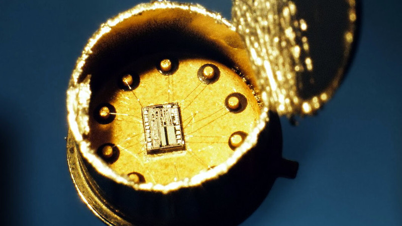
Metal can sawn open image: Dub [CC0].


I would argue that Q1 and probably Q9 are also part of the Differential Amp. Q1 is the “constant current source” Q2 and Q3 need to do their work.
Isn’t that what I said?
Is it bad that I knew it was Bob Widlar’s design from remembering the part number from that wonderful article about him from 2014?
Bob Widlar
https://en.wikipedia.org/wiki/Bob_Widlar
https://hackaday.com/2014/04/08/heroes-of-hardware-revolution-bob-widlar/
Wow! Interesting read!
I agree …as a young Radio & TV apprentice in the late 60’s, I used to eagerly look forward to receiving a large envelope here in NZ all the way from Fairchild, containing their latest data sheets. Even though some of it was beyond me at the time…I recognised that I was looking at cutting edge development and I followed every step that Fairchild made. Those were the days….as the words of the old song go. Today at the ripe old age of 78, I still feel in touch with the spirit of Fairchild and their engineers when I buy my semiconductors from China, still with the big F on the package.
GREAT post.
Thanks!
gain = -Rf/Ri
I’m getting that tattoo fixed right after I edit this post. Dangit.
Oops! Sorry.
Don’t forget Bob Pease.
He’s pictured in this story:
https://www.edn.com/electronics-blogs/anablog/4311277/Bob-Widlar-cherry-bombs-the-intercom-speaker-item-2
Here’s the hard-to-find Robert A. Pease story about Bob Widlar:
https://web.archive.org/web/20130216053224/http://portal.national.com/rap/Story/widlar.html
These guys were hackers of the most obstinate and difficult kind. Pease told me, shortly before his unfortunate demise, how much he preferred doing work with analog circuitry rather than digital. Years before, when Pease was working for Analog Devices he was doing a lot of hiking in the White Mountains of New Hampshire, which is how I encountered him. His specialty was tracing former paths of AMC trails that had been relocated.
My mistake. Pease did not work at Analog Devices, even though it was about three miles from his home. Instead he worked for Philbrick.
WordPress got my ALT-NAME ALT-ALIAS ALT-wrong by misteak.
The 702 was a shitty opamp. But it was the only monolithic opamp in 1964, and they could sell it for $300. You could buy a nice TV set for that price in 1964.
But then they made the 709, which was not bad. That thing sold like hotcakes, and pretty much gave Fairchild a license to print money, at least for a few years.
Agreed. But the 702 is simple, which makes it ideal for an exploration of op-amp internals.
“That thing sold like hotcakes, and pretty much gave Fairchild a license to print money, at least for a few years.”
That would be about the time the engineers started jumping ship and forming all of the Fairchildren.
I did EMP testing on 709s, and delidded them all to see what smoked. I charged up a piece of 3-1/8 inch rigid coax to ten or 20 KV and discharged through a small thyratron. I took data on a scope camera with polaroid film. They took a lot more voltage than 741s, and subsequent chips had smaller transistors still, so easier to kill.
OK, I’m mostly a digital guy so someone with better analog chops than mine please explain pin 1 (ground) to me, I looked up the datasheet, and even pulled out my olde Horowitz and Hill MK-II and I still can’t quite see how this is supposed to work.
I can see where Q5 is an emitter follower off one leg of the differential pair and it mostly buffers the signal to Q6 but why tie the Q5 emitter to ground? I can see where that sets the level shift, but with the emitter of Q5 at ground that leaves the base of Q5 at .7v, which is tied to the collector of Q3. Same with Q4/Q2. This means that Q2/Q3 stops working as a differential pair whenever the base of one of them gets above a few fractions of a volt (since a bipolar transistor needs a minimum Vcb to stay in the linear region, and all bets are off anyway if Vb exceeds Vc).
If you’re always using this part as a vanilla inverter I suppose that’s OK, since you’re going to tie V- to ground and virtual ground will keep V+ within millivolts, but for any application that involves common mode voltage (or at least positive common mode voltage) like a non-inverting amp or a voltage follower, I don’t see how this works.
Good observation. This is one of the things that made this a lousy amp. It had a input common mode range of .5v min and 1v typical- see data sheet. In the minus direction it did a little better. Look at the 709 where Widlar fixed this stuff. The assumption is its a low level amp. We’re spoiled by all this near rail to rail stuff.
Well, it simply doesn’t. That thing is, as stated above, not a particularly good Op amp. But it is the first (monolithic).
Don’t mind me, just here to make a pun.
A pun what subject?
Doxology.
I skated right into that one!
B^)
Q5 is an common emitter amplifier rather than an emitter follower. R7 just provides current for the low-side current sources Q9-Q1-Q8.
Q4 holds Q2’s collector voltage at a nearly constant value, forcing almost all the voltage change on R1 and R2 to appear at the collector of Q3, basically doubling Q3’s voltage gain. Q5-R4 match Q4-R3 so Q2 and Q3 see nearly identical loads, which improves linearity and offset voltage.
Q5 provides a second stage of voltage gain driven from Q3’s collector, and the output at its collector drives level-shifted Darlington output Q6-Q7.
If you set pin 1 one Vbe below the average input voltage, it holds the average collector voltage of Q2 and Q3 near the input voltage, which reduces input leakage current through the bases of Q2 and Q3, and reducing drift.
The design is suitable for inverting applications where the positive input is connected to a constant voltage (usually GND) and the feedback network keeps the negative input from going more than a few microvolts away from the positive input.
It isn’t the greatest op amp ever made, but most people would have a hard time designing something as good from scratch using only resistors and NPNs.
Lets just day that even though its crude and nowhere near as good as discrete amps of that era (which were 100 times the size), Widlar had a clue… when all his peers, at the time, were nearly clueless (or had trouble getting funded).
Anyone who hasn’t seen this: Do it now!
https://www.youtube.com/watch?v=sxwMVJeQ4Ps
The story of Robert Noyce and how he created the modern world.
Here how an other iconic Op-Amp works. It is explained in great detail. I hope you enjoy it.
https://youtu.be/A0wn_SrZzeo