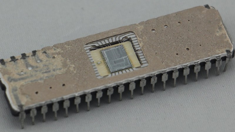
Even with ten fingers to work with, math can be hard. Microprocessors, with the silicon equivalent of just two fingers, can have an even harder time with calculations, often taking multiple machine cycles to figure out something as simple as pi. And so 40 years ago, Intel decided to give its fledgling microprocessors a break by introducing the 8087 floating-point coprocessor.
If you’ve ever wondered what was going on inside the 8087, wonder no more. [Ken Shirriff] has decapped an 8087 to reveal its inner structure, which turns out to be closely related to its function. After a quick tour of the general layout of the die, including locating the microcode engine and ROM, and a quick review of the NMOS architecture of the four-decade-old technology, [Ken] dug into the meat of the coprocessor and the reason it could speed up certain floating-point calculations by up to 100-fold. A generous portion of the complex die is devoted to a ROM that does nothing but store constants needed for its calculation algorithms. By carefully examining the pattern of NMOS transistors in the ROM area and making some educated guesses, he was able to see the binary representation of constants such as pi and the square root of two. There’s also an extensive series of arctangent and log2 constants, used for the CORDIC algorithm, which reduces otherwise complex transcendental calculations to a few quick and easy bitwise shifts and adds.
[Ken] has popped the hood on a lot of chips before, finding butterflies in an op-amp and reverse-engineering a Sinclair scientific calculator. But there’s something about seeing constants hard-coded in silicon that really fascinates us.


The Parallax Propller has a CORDIC Engine built into it as well. Going on 20 years old I’m suprised no one has noticed this in the Parallax Proip.
I;m just amazed that no one has added such a CORDIC Engine to FPGA implementations of CPU’s.
Few CPUs have instructions needing CORDIC : trigonometric, exponentials. Mainly the x87 and MC68881/2.
Divisions and square root have faster algorithms and RISCs prefer software implementations.
Even the x86 family replaced CORDIC with numeric suites in later models (around 387 or i486). For a fast FPU, implementing fast addition and multiplication is more important than transcendentals, and once there is a fast multiplier around (or mul-add), numeric suites are faster than CORDIC.
Still, CORDIC is a neat algorithm.
Very cool information, thank you!
There was the AMD 9511 math processor which existed before the 8087. As I recall, more complicated to interface, and not a coprocessor. But it worked with various CPUs.
There were also a couple of articles about interfacing a Mos Technology calculator to a microprocessor, I’m not sure if the device was aimed at the task or just an off the shelf calculator IC.
Very slow, but probab!y faster than doing the floating point on the CPU, and it beat writing floating point routines.
The 9511 (or -12; I forget — one of them was BCD) was a great chip. We were designing 8086-based things back then and we needed some faster math. Looked at the 8087 and discovered that the 8086 got stalled and just waited while the ’87 did its thing (‘cos both shared the same memory and bus), so the time improvement was fairly minimal. The AMD chip could be given a fairly complicated problem to solve (it had a stack, IIRC), and it would go off and do it, generating an interrupt when it got the answer. Much more efficient.
Am9511 was a truly fascinating chip… I always wondered about its internals, but it is certain it is driven by some complex microcode worth reverse engineering even after all these years. It could make a for a cool FPGA implementation, running at least 10-20 times faster than the original. I played with it a bit: https://github.com/zpekic/am9511
“There was the AMD 9511 math processor which existed before the 8087.”
Yes, there was. Here’s a photo I took of it:
https://live.staticflickr.com/65535/49918929753_35f5fadb54_k.jpg
A macro photo of its die, not of the IC package, BTW.
Fascinating chip… The constants are on top left, the microcode on bottom right, and the registers on top center (appears like a 8*16 structure, which is the size of internal stack). But the mystery is the register block on the center left, which also appears like a 8*16. If so, then perhaps the register stack appears as two blocks, facilitating simultaneous feeding of 2 operands into the ALU, and on the update path both are written (a variation of the dual – port RAM implementation).
From the article:
> The chip’s data path consists of 67 horizontal rows, so it seemed pretty clear that the 134 rows in the ROM corresponded to two sets of 67-bit constants. I extracted one set of constants for the odd rows and one for the even rows, but the values didn’t make any sense. After more thought, I determined that the rows do not alternate but are arranged in a repeating “ABBA” pattern.
Mama Mia, who thought of that?
Haha, nice one!
I think it was some guy named Fernando
I remember using the 8087 in a tracking radar system. It didn’t denormalise properly as a number reduced toward zero. This caused us some serious headaches until we found out what was going on
“Microprocessors, with the silicon equivalent of just two fingers”
You mean one finger? Trinary isn’t common since silicon came along, and I don’t think it was used in a 808x.