Going On A Tangent With The Intel 8087’s Hybrid CORDIC Algorithm

Continuing their reverse-engineering of Intel’s 8087 FPU, [Ken Shirriff] and friends took a look at one of the trigonometric functions, specifically FPTAN.  The most exciting part with such reverse-engineering is probably figuring out which algorithm was used in the implementation, while trying to determine the reasoning behind the final hardware design.

If you’re running a simple MCU or MPU like the 6502 or Z80 without hardware functions you’d likely use an algorithm such as CORDIC or similar, as this requires only basic hardware features like addition, subtraction, bitshift, and look-up tables. One can also use polynomial approximation if there’s hardware support for a potential speed-up, or as is the case in the 8087, create a hybrid approach that targets speed and accuracy.

In the article the exact implementation to get to 64 bits of accuracy is detailed, starting with the 16 bits calculated using CORDIC before switching to the Padé approximant technique involving the ratio of two polynomials. Since after calculating the brunt of the final value with CORDIC the remainder is a fairly small value, this polynomial approximation is not just very accurate but also fast.

This approach allows the FPTAN and similar trigonometric functions in this FPU to hit a very high level of accuracy and not require the look-up table sizes and additional time required to work through the remaining bits with CORDIC. For those who want to see the full algorithm Intel’s engineers used, [Ken] has the full microcode listing with comments in the article as well.

As for the exact speed-up from this approach, [Ken] calculates for one value that FPTAN would spend 33% on CORDIC pseudo-division, 47% on CORDIC pseudo-multiplication and a mere 15% on the polynomial approximation along with about 5% overhead.

With the Pentium series of CPUs Intel moved completely away from CORDIC, as it’s clear that as accurate as it may be, it’s hard to scale to a significant number of bits without incurring significant time penalties. With the introduction of SIMD instructions the x87 ISA has further seen its functionality reduced, but this analysis shows once again why the 8087 made such an impact when it was released.
How The Intel 8087 FPU Knows Which Instructions To Execute

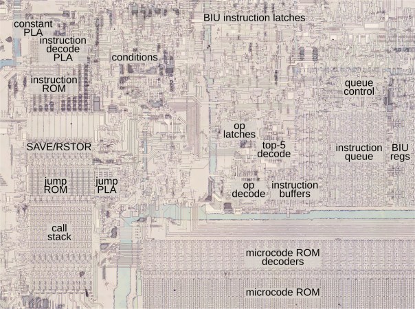
An interesting detail about the Intel 8087 floating point processor (FPU) is that it’s a co-processor that shares a bus with the 8086 or 8088 CPU and system memory, which means that somehow both the CPU and FPU need to know which instructions are intended for the FPU. Key to this are eight so-called ESCAPE opcodes that are assigned to the co-processor, as explained in a recent article by [Ken Shirriff].

The 8087 thus waits to see whether it sees these opcodes, but since it doesn’t have access to the CPU’s registers, sharing data has to occur via system memory. The address for this is calculated by the CPU and read from by the CPU, with this address registered by the FPU and stores for later use in its BIU register. From there the instruction can be fully decoded and executed.

This decoding is mostly done by the microcode engine, with conditional instructions like cos featuring circuitry that sprawls all over the IC. Explained in the article is how the microcode engine even knows how to begin this decoding process, considering the complexity of these instructions. The biggest limitation at the time was that even a 2 kB ROM was already quite large, which resulted in the 8087 using only 22 microcode entry points, using a combination of logic gates and PLAs to fully implement the entire ROM.

Only some instructions are directly implemented in hardware at the bus interface (BIU), which means that a lot depends on this microcode engine and the ROM for things to work half-way efficiently. This need to solve problems like e.g. fetching constants resulted in a similarly complex-but-transistor-saving approach for such cases.

Even if the 8087 architecture is convoluted and the ISA not well-regarded today, you absolutely have to respect the sheer engineering skills and out-of-the-box thinking of the 8087 project’s engineers.

The Intel 8087 And Conditional Microcode Tests

Continuing his reverse-engineering of the Intel 8087, [Ken Shirriff] covers the conditional tests that are implemented in the microcode of this floating point processing unit (FPU). This microcode contains the details on how to perform the many types of specialized instructions, like cos and arctan, all of which decode into many microcode ops. These micro ops are executed by the microcode engine, which [Ken] will cover in more detail in an upcoming article, but which is effectively its own CPU.

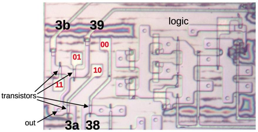
Conditional instructions are implemented in hardware, integrating the states of various functional blocks across the die, ranging from the instruction decoder to a register. Here, the evaluation is performed as close as possible to the source of said parameter to save on wiring.

Implementing this circuitry are multiplexers, with an example shown in the top die shot image. Depending on the local conditions, any of four pass transistors is energized, passing through that input. Not shown in the die shot image are the inverters or buffers that are required with the use of pass transistors to amplify the signal, since pass transistors do not provide that feature.

Despite how firmly obsolete the 8087 is today, it still provides an amazing learning opportunity for anyone interested in ASIC design, which is why it’s so great that [Ken] and his fellow reverse-engineering enthusiasts keep plugging away at recovering all this knowledge.

Reverse-Engineering The Intel 8087 Stack Circuitry

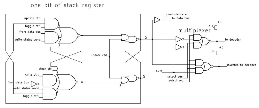
Although something that’s taken for granted these days, the ability to perform floating-point operations in hardware was, for the longest time, something reserved for people with big wallets. This began to change around the time that Intel released the 8087 FPU coprocessor in 1980, featuring hardware support for floating-point arithmetic at a blistering 50 KFLOPS. Notably, the 8087 uses a stack-based architecture, a major departure from existing FPUs. Recently [Ken Shirriff] took a literal closer look at this stack circuitry to see what it looks like and how it works.

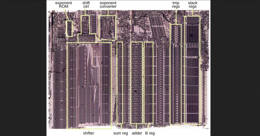
Nearly half of the 8087’s die is taken up by the microcode frontend and bus controller, with a block containing constants like π alongside the FP calculation-processing datapath section taking up much of the rest. Nestled along the side are the eight registers and the stack controller. At 80 bits per FP number, the required registers and related were pretty sizeable for the era, especially when you consider that the roughly 60,000 transistors in the 8087 were paired alongside the 29,000 transistors in the 16-bit 8086.

Each of the 8087’s registers is selected by the decoded instructions via a lot of wiring that can still be fairly easily traced despite the FPU’s die being larger than the CPU it accompanied. As for the unique stack-based register approach, this turned out to be mostly a hindrance, and the reason why the x87 FP instructions in the x86 ISA are still quite maligned today. Yet with careful use, providing a big boost over traditional code, this made it a success by that benchmark, even if MMX, SSE, and others reverted to a stackless design.

A Forgotten Consumer PC Becomes A Floating Point Powerhouse

[Michael Wessel] found some of his old DOS 3D graphics software and tried to run it on an 8088 PC. The tale of adding an 8087 co-processor to speed up the rendering was anything but straightforward, resulting in a useful little project.

There was a point around the end of the 1980s when the world of PCs had moved on to the 386, but the humble 8086 and 8088 hung around at the consumer end of the market. For Europeans that meant a variety of non-standard machines with brand names such as Amstrad and Schneider, and even surprisingly, later on Sinclair and Commodore too.

Of these the Schneider Euro PC was an all-in-one design reminiscent of an Amiga or Atari ST, packing a serviceable 8088 PC with a single 3.5″ floppy drive. A cheap machine like this was never thought to need an 8087, and lacked the usual socket on the motherboard, so he made a small PCB daughter board for the 8088 socket with space for both chips.

It’s a surprisingly simple circuit, as obviously the two chips were meant to exist together. It certainly had the desired effect on his frame rate, though we’re not sure how many other Euro PC users will need it. It does make us curious though, as to how quickly a modern microcontroller could emulate an 8087 for an even faster render time. Meanwhile if you’re curious about the 8087, of course [Ken Shirriff] has taken a look at it.

Looking For Pi In The 8087 Math Coprocessor Chip

Even with ten fingers to work with, math can be hard. Microprocessors, with the silicon equivalent of just two fingers, can have an even harder time with calculations, often taking multiple machine cycles to figure out something as simple as pi. And so 40 years ago, Intel decided to give its fledgling microprocessors a break by introducing the 8087 floating-point coprocessor.

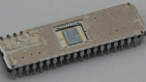
If you’ve ever wondered what was going on inside the 8087, wonder no more. [Ken Shirriff] has decapped an 8087 to reveal its inner structure, which turns out to be closely related to its function. After a quick tour of the general layout of the die, including locating the microcode engine and ROM, and a quick review of the NMOS architecture of the four-decade-old technology, [Ken] dug into the meat of the coprocessor and the reason it could speed up certain floating-point calculations by up to 100-fold. A generous portion of the complex die is devoted to a ROM that does nothing but store constants needed for its calculation algorithms. By carefully examining the pattern of NMOS transistors in the ROM area and making some educated guesses, he was able to see the binary representation of constants such as pi and the square root of two. There’s also an extensive series of arctangent and log2 constants, used for the CORDIC algorithm, which reduces otherwise complex transcendental calculations to a few quick and easy bitwise shifts and adds.

[Ken] has popped the hood on a lot of chips before, finding butterflies in an op-amp and reverse-engineering a Sinclair scientific calculator. But there’s something about seeing constants hard-coded in silicon that really fascinates us.

8087's -5V bias charge pump circuit

How The 8087 Coprocessor Got Its Bias

Most of us have been there. You build a device but realize you need two or more voltages. You could hook up multiple power supplies but that can be inconvenient and just not elegant. Alternatively, you can do something in the device itself to create the extra voltages starting with just one. When [Ken Shirriff] decapped an 8087 coprocessor to begin exploring it, he found it had that very problem. It needed: +5 V, a ground, and an additional -5 V.

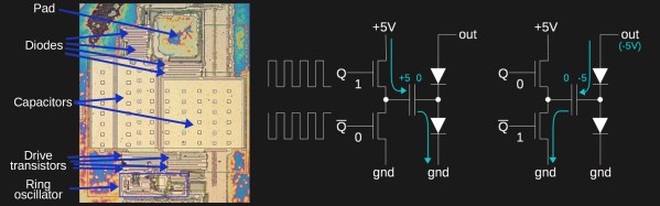
His exploration starts with a smoking gun. After decapping the chip and counting out all the bond wires going to the various pads, he saw there was one too many. It wasn’t hard to see that the extra wire went to the chip’s substrate itself. This was for providing a negative bias to the substrate, something done in some high-performance chips to get increased speed, a more predictable transistor threshold voltage, and to reduce leakage current. Examining where the bond wire went to in the circuitry he found the two charge pump circuits shown in the banner image. Those worked in alternating fashion to supply a -5 V bias to the substrate, or rather around -3 V when you take into account voltage drops. Of course, he also explains the circuits and dives in deeper, including showing how the oscillations are provided to make the charge pumps work.

If this is anything like [Ken’s] previous explorations, it’ll be the first of a series of posts exploring the 8087. At least that’s what we hope given how he’d previously delighted us with a reverse engineering of the 76477 sound effects chip used in Space Invaders and then went deeper to talk about integrated injection logic (I2L) as used in parts of the chip.