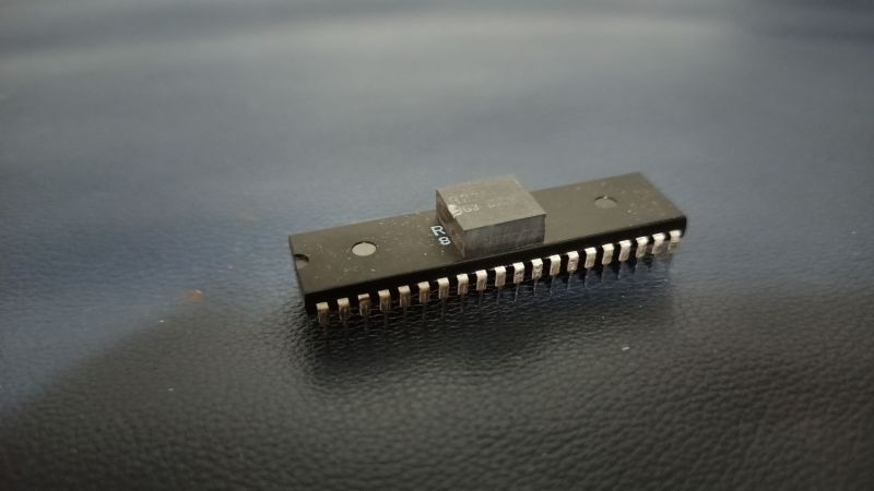
At least by today’s standards, some of the early chips were really, really big. They may have been revolutionary and they certainly did shrink the size of electronic devices, but integrating a 40-pin DIP into a modern design can be problematic. The solution: cut off all the extra plastic and just work with the die within.
 When [Redherring32] alerted us to this innovation, he didn’t include much information — just a couple of photos of the mod and a few brief words about the target chip, an RP2A03 from the glorious NES 8-bit days. Living as it does within the relatively enormous DIP-40 package, it stood to take up far too much space in compact, more modern designs. So the hapless chip fell under the knife, or rather the Dremel tool diamond cutoff wheel. [Redherring32] left a generous boundary around the die. Cutting through the package left the lead frame of the die exposed enough to solder 34AWG (0.02 mm²) magnet wire to bring the leads out for connection. We’d have worried that vibration from the cutting process would have damaged the silicon, but the video in the tweet tells otherwise.
For now, the liberated die is connected to a piece of perfboard, which ironically enough actually makes it larger than the original chip. But this is a proof-of-concept, and given that the operation shrunk the footprint of the chip by about 93%, it should enable some interesting applications. Perhaps a smaller, better version of [Redherring32]’s OpenTendo is in the works.


That’s really cool. Just make a custom footprint for it and surface mount it on your custom pcb.
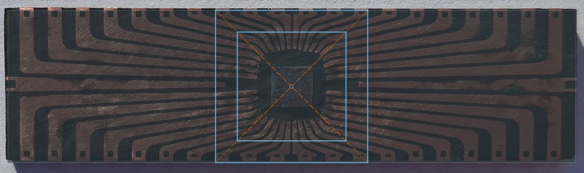
The photo with the entire lead frame visible is just for illustration. The chip probably wouldn’t work anymore with that done to it. The actual dremeled chip has the same thickness and small rectangular patches of exposed copper on the sides.
Thinking outside the box 101. Well done.
Building a better box.
Awesome.
I suggested this for the N64 (https://hackaday.com/2020/12/25/is-this-the-worlds-smallest-nintendo-64/#comment-6306082) but the NES is a better choice.
A block off the ol’ chip.
You can do something similar with modern DIP AVR chips. Cut the ends off and use GPIO pins to power the chip through the protection diodes.
Let Benheck know he can start working on his Atari in an altoids tin/Dreamcast VMU XD
https://www.westerndesigncenter.com/wdc/w65c02s-chip.php#thumb
Wrong chip. The 6502 isn’t going to contain the DAC, the APU, or the video timing hardware inside of it.
It even gives you A14 and A15 to use externally, so it can’t possibly have the extra hardware inside that uses that IO space.
W65C02S6TPLG-14 8-bit Microprocessor in a 44 Pin PLCC package
65816 as well.
They don’t have the 2A03 APU on die though, so not much use for NES.
okay…. so cut the CPU down to size… then spent all day soldering it to a giant FR4 portoard with pinheaders ?
am i missing something
Perfboard was only to test that it was still functional.
Thank you for explaining that. I had the same objection, but now it makes sense :)
Before you slice up a chip though, many of them were available as dies for integrating into hybrid modules, so you could try a search to source NOS dies.
Good idea but not everyone have an die wire bonding machine.
Isn’t it just the world’s tiniest spot welder? We know how to make spot welders in these parts. Unless you need unobtainium wire to achieve the bond w/o wrecking the die, sounds like a fun and pointless way to spend a Saturday afternoon. Would recommend practicing on something cheap like a Z80
The bondwire is (excluding exotic methods) normally welded with a combination of heat and ultrasound. Probably not too difficult to improvise a machine that can make a wirebond if you are good with metalworking, but making a practical one with sufficient precision will be hard I think. You often find old ones on the surplus marker though, for these old dies they should be more than enough
Maybe the next level for this is to build the NES in as small a 3d volume as possible. You’d have to wire up in layers. It would be wonderful to see a real compact ‘dead bug’ NES!
How hardware-authentic do you need the thing to be?
Emulating a NES on a 32 bit MCU isn’t that uncommon, see for example the Odroid Go[1] (which in the end runs an ARM cortex-M port of [2]), and considering MCUs like the one used in that only need small amounts of power, you’re adding maybe two digits of mm³ in power supply, and mono headphone amplifier, you’d be waaaay under 1 cm³ if you really really really wanted to squeeze this down. Sandwiched <0.6mm thick PCBs, 0201 (or smaller) passives and QFN or even (WL)CSP make this possible – after all, your smart phone contains a desktop-grade computer, batteries, display, very-many-bands-and-protocols wireless interface, and a lot of auxiliary sensors that a minimal implementation of something that plays NES games doesn't need.
If you don't care about things like access to external memory, can live with unamplified sound, and if you have a power source that's sufficient for one, I think most realistically, the answer to the question "how small do I get a NES game-running system" is "your connector for a NES controller has 100× the volume of a CSP ARM cortex-M0+/-M4 with megabits of flash and RAM, why are we even talking about this?
If you're, however, insisting on an actual 6502 core (instead of just its instruction set) with the main (sound, graphics) peripherals happening in hardware, well the question then slims down to "would you like to do microcode emulation on a soft-CPU in an FPGA, or implement one of the dozens of 6502 cores directly in the FPGA", and then you'd pick one of the rather small FPGAs. This is really really really well-understood old tech, and we can reconstruct it within new tech.
Let's get a feeling for how big things will be.
This has been done before, for example by Jonathan Sieber (writeup: [1], Source code: [2], Presentation: [3]), and if you look through his documentation, you'll find he's used a little more than 4000 LUTs of the Virtex 5 he had. The Virtex 5, albeit oldish, is really quite beefy (each slice has four of these 6-input LUTs, which makes them quite potent in terms of representing complex logical functions), but let's say two 4-LUTs are equivalent to one 6-LUT in practice (just to get something like a likely upper bound), so, 8000 4-LUT FPGAs would suffice, like the smallest Lattice ECP5 still does (by a factor of 1.5, I'd like to add), and there's higher-slice-count ECP5s in the same 10mm×10mm package (which atop of that is also relatively forgiving to solder with its large pitch, allowing for realistically cheap 4-layer PCBs with passives directly below). So, add in 2 cm² for power and 1 cm² for interconnect incl audio, you've got a 4 cm² NES that's only missing a connector to plug in your controller and screen, at a height that's below 6mm, including PCB. So, at this level of "my hardware actually *is* the 6502 with its specific "interesting" peripheral choices, 2.4 cm³ is my estimate for "How small can I make a fully functional NES".
[1] https://wiki.odroid.com/odroid_go/odroid_go#hardware
[2] https://www.zophar.net/nes/nofrendo.html
[1] https://entropia.de/images/4/47/GPN13-Nintendo_Entertainment_System_on_FPGA.pdf
[2] https://github.com/strfry/nesfpga
[3] http://ftp.ccc.de/events/gpn/gpn13/gpn13-nes-fpga.mp4
Did a 6502 soft core in a Spartan6 LX9 with room to spare. That was 7 years ago, so how much room to spare? Idk, seemed like about half, maybe a bit more.
just optimize your code even more and you might have a full byte to spare.
sorry…
Just get an old wire bonder and make it into a SOI or TQFP :-P
In theory you could sand it thinner than it is, but that would be a little nerve wracking.
Just put the cut down chip into a PLCC44 chip adaptor [ or a PLCC32 and add jumpers ], then fill it with apoxy, to keep it a little more mechanically stable. If you left a bit more of the legs on it, you wouldn’t need to solder the magnet wire, just bend them around the remains of chip, alternating up and down so they are less likely to touch. Perhaps soldering then into the chip holder if required.
The leadframe material is pretty resistant to bending: it cracks without a generous bend radius. I’ve tried this.
Not sure about this. Ok, you will gain some space, but you will spent quite a lot of funny time soldering tiny tiny wires to tiny tiny leads and thats not fun at all. So…
What about chip cooling? Those 2 straps that goes strait at each end of the DIP-40. These are heat sink. It is not apparent on the photo but they are linked to the die to dissipate heat.
This was my concern as well.
I also had the same concern, however after running it a few hours it hasn’t gotten any warmer than normal so it doesn’t appear to be an issue.
I was wondering the same. You could always integrate cooling tracks and vias in the PCB instead.
Chips back then don’t get very hot anyway. The “2 straps” are just part of the lead frame and have nothing to do with being heatsink. They are rather useless as heatsink the die is not attched to them.
I wonder if you’d be better off attaching the chip unmodified, to your main board, but dead bug style, across other components. Then solder wires to a common area. So long as the overall board is larger than the chip, you are not gaining much by cutting it down. If height is a concern, you could cut the pins short as well, without completely removing them, but soldering to the cut pins is going to be a heck of s lot easier than this mod.
I think you are headed in the right direction. Now make it an IC socket rather than the IC itself and you’ve got it.
Actually, rather than dead bug style maybe an IC socket with really long legs could be found and mounted over top the other components like a tent.