Do you need a microcontroller that runs at 1 GHz? No, probably not. But that didn’t stop [Visual Micro] from trying, and the results are pretty interesting. Not only did the plucky little chip not cook itself, it actually seemed to run fairly well; with the already powerful microcontroller getting a considerable boost in performance.
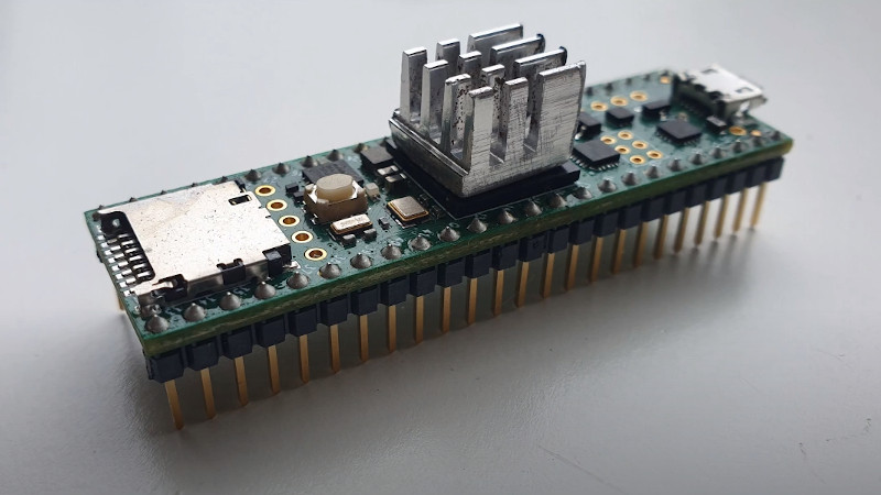
According to [Visual Micro] the Teensy 4.1, which normally has its ARM Cortex-M7 clocked at 600 MHz, can run at up to 800 MHz without any additional cooling. But beyond that, you’ll want to invite some extra surface area to the party. It’s easy enough to cut a chunk out of an old CPU/GPU cooler and stick it on with a dab of thermal compound, but of course there’s no shortage of commercially available heatsinks at this size that you could pick up cheap.
With the heatsink installed, [Visual Micro] shows the Teensy running at around 62 °C during a benchmark. If that’s a little hot for your liking, they also experimented with an old laptop cooler which knocked the chip down to an impressive 38 °C while under load. It doesn’t look like a particularly practical setup to us, but at least the option is there.
[Visual Micro] unfortunately doesn’t go into a lot of detail about the benchmark results, but from what’s shown, it appears the overclock netted considerable gains. A chart shows that in the time it took a stock Teensy to calculate 15.2 million prime numbers, the overclocked chip managed to blow through 21.1 million. The timescale for this test is not immediately clear, but the improvement is obvious.
Even at the stock 600 MHz, the Teensy 4 is a very powerful MCU. Especially after the 4.1 refresh brought in support for additional peripherals and more RAM. But we suppose some people are never satisfied. Got a project in mind that could benefit from an overclocked Teensy? We’d love to hear about it.
Thanks to [Zane] for the tip.


please continue to justify my belief that the teensy is too op for most applications.
Every single microcontroller ever made is too {fill in the blank} for the {fill in the blank} application. This is why they come in such a wide variety.
I don’t know, you can always go blankier.
To make it a bit tautological: the classic applications for an 8-bit microcontroller still only require an 8-bit microcontroller. That’s why PICs stayed around forever.
Not worse than the people using RPi 3’s for a wifi-enabled curtain. an 8266 doesn’t feel too overpowered for that application even though it has way more power than needed
I burned Tensorflow Lite on Teensy 4 and 4.1, and they ran pretty well on FP32 precision.
The Arduino IDE has a 1GHz clockspeed setting for the Teensy 4.
I requires a cooler on the MCU but nothing more fancy than that.
If you do not want to overclock, then take a look at the newer family version of the chip the Teensy 4 uses, as this new family (RT117x) clocks at 1 Ghz out of the box. Additional the RT117x family includes two cores (M7 and M4) and is an absolute screamer with all the goodies it offers for the price (I bought a tray of the RT1176’s for about $8 US ea.). For those that say why does one need to performance… well, on price alone it can be far less expensive using it than some older devices.
the price disparity between “low powered” and “overpowered” is genuinely fascinating and funky. there’s a lower flatline for DIP chips which are nicer for prototyping, but most of the cost of a dev board is the board itself, not the chip. but then you get into the tradeoffs: Arduino is very polarizing, but it’s accessible and the amount of invested time-labor means it’s very likely that [obscure task] has already been done, at least two different ways. it gets harder to find that same breadth of value in other chips such as STM34F4nn, which I have not (yet) found a working USB HID Joystick library for (and I’m not clever/patient enough to try and port MHeironymous’s work to another chiparch even inside the Arduino IDE)
Dang I couldn’t find any of these when I looked last. That said I never had a problem running it at 975mhz.
What you using for bootloader? Where did you find the chips? I haven’t looked in 3 or 4 months but all 117x were showing like 1 year lead time.
That’s the chip shortage for you.
Teensys are pretty cheap, why not just submerge it in an mineral oil bath for liquid cooling?
Now do a 555 timer.
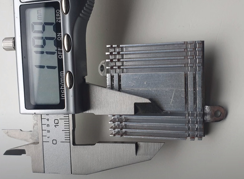
The heatsink is from a PC motherboard north bridge chip. In case you looking for one.
I just used pi heatsinks.
It’s an ARM processor. Most of us carry around ARM processors that run at multiple GHz. It’s an 6-stage superscalar pipeline with branch prediction.
I would love to see the hackiness of someone getting an 8-bit AVR or PIC instruction set running at 1 GHz. It would probably take implementing it in an HDL and running it on a pretty advanced FPGA, because the smaller ones can’t clock that high, regardless of the number of pipeline stages.
Even the highest end FPGAs can’t run fabric at 1 GHz, and with simpler instruction sets, they’re not pipelined so you’d never be able to run them that fast regardless of tricks.
Even at 500 MHz you can barely do anything.
I never understood why a pipeline is needed for higher frequencies. A 6502 needs an average of 4 cycles per instruction. So clocked with 1GHz, wouldn’t it mean 250Mips?
Without pipelining a processor has to execute the entire instruction in a single clock cycle. That takes a while so the processor can’t run at a very high frequency. So they split up each instruction into multiple stages of execution and each stage takes less time than the whole instruction. Your 6502 example actually does this, in each cycle the 6502 is processing a different part of the instruction. The entire instruction still takes the same amount of time overall to execute so you’re still achieving 250Mips but the possible clock frequency is 4 times higher. Here’s why they do that:
Firstly this makes instructions such as i=i+1 sensical. Let’s say the instruction is split into 4 stages: decode instruction, read cpu register, do math, write cpu register. If this was done all at once like it is in formal math then you create a feedback loop where 1 is added to i as many times a clock as the circuitry allows until the next clock pulse and the next instruction is executed. But if you separate the stages and only perform one on each clock then 1 is only added to i once.
The other reason and the one that leads to performance improvement is this. Our instruction may take the same amount of time to execute as if it wasn’t split into stages but it’s only undergoing one stage at a time. So you can use the other parts of the “pipeline” to execute different stages of other instructions at the same time. This means that our four stage pipeline is actually executing 4 instructions at the same time and finishing one every clock. At 1 GHz you’re no longer getting 250Mips, but a full 1Gips!
Thanks for the explanation!
There’s a similar pipeline on fast ADC’s.
In the first stage, 16 comparators give 4 bits output. The sample moves to a second stage where another 16 comparators produce another 4 bits of resolution, while the first stage starts processing the next sample.
3 stages give a high sample rate, with a 12-bit sample taking just 3 clock cycles to process.
@[Alan]
An excellent example.
If I skip the 6502 as it is already kind of pipelined with the phase pin.
So I’ll go with the Z80 which was a CISC from the same era. However I will ignore the refresh phase.
I’ll start at the end! because well there isn’t really a beginning or end.
So here we go:
The address bus has an address, the write signal is asserted and the data bus has the data that has just been written to that address.
The address bus is connected to the output of the “HL” register pair (16 bits) and the data bus is connected to the output of the “A” register (8 bits).
These internal to external connections HL => address bus and A => data base are being held in place buy the instruction decode logic that has decoded the instruction LD (HL),A – or load the contents of the A register into the memory location pointed to by the contents of the HL register pair.
The PC (Program Counter) has just finished incrementing and the CPU is about to load the next byte into the instruction register.
How fast the chip can go is determined by the time (propagation delay) it takes for all of the states (in order) to settle into a temporary static state. The instruction decoder had to enable the internal and internal to external connections. These connections take time to establish then there are delays with other aspects like the memory being ready to read or write and the time it takes for that process to complete and other things that I deliberately didn’t mention like the ALU because I wanted to make a simple case. Sufficient to say there are many many of these delays at every stage and they all add up.
This is a “JUST in Time” Timing Scheme. And if you look at the Z80 timing diagrams you will see what a nightmare it is to conform to this timing scheme with the hardware or at least working out how to.
Anyway, the bottom line is that everything reaches a static state waiting for the process to complete. At the end of the instruction when the instruction is completing as it loading something to or from memory or whatever the decode logic is sitting there holding a static state as the rest of the process is dependent on that.
The downside is that except for the current stage all that silicon is doing nothing.
Many instructions can be broken down into sub processes. For example –
1) Instruction Fetch.
2) Instruction Decode.
3) Read Memory
4) ALU Operations
5) Write (result) to memory.
Pipelining.
Now if the instruction fetch logic latches its state it can start loading the next instruction while the Instruction decode is deciding what to do with the first instruction.
So, simply, if you have sets of latches between stages then you can have every stage working all the time instead of the whole lot waiting for one instruction to complete.
The net effect is that (if you have 4 stages) then your “Effective” CPU speed is approximately 4 times what it was, minus a bit of extra propagation delay for the extra latches between stages.
In reality it’s a little more complex as not all instructions have the same number or combination of sub-processes especially a CISC CPU.
Another complication is that anything that represents the common “If” in programming languages has to flush the pipeline and start at a different memory location – depending on “true” or “false”.
CISC processors like the 6502 or Z80 are not easy to pipeline as they have complex instructions that vary in processing length. But it can be done.
RISC processors are much easier.
Then there are specific architectures like “Read Modify Write” that are perfect for pipelining. Some architecture are specifically designed for pipelining.
So pipelining is about breaking instructions down into sub-processes, designing logic for each sub-process, putting latches between each sub-process so that all the silicon is working on different instructions (in order) instead of it all waiting for the current (first) instruction to complete.
Of course this increases power consumption and thermal dissipation.
Cool, thx
FPGA is generally rated by the pin to pin propagation.
In my experience with cheaper CPU’s the higher the rated clock speed, the less it is correlated to actual instruction execution speed.
What, no water cooling?
We tried it with some “simplistic” water cooling shall we say, with good results. Of course we could add a proper water cooled heatsink and radiator system…. or maybe some dry ice :-)
https://www.youtube.com/watch?v=ddobxixfRyA
So you want a project that uses an overclocked teensy..guess it’s time to upload something to github.