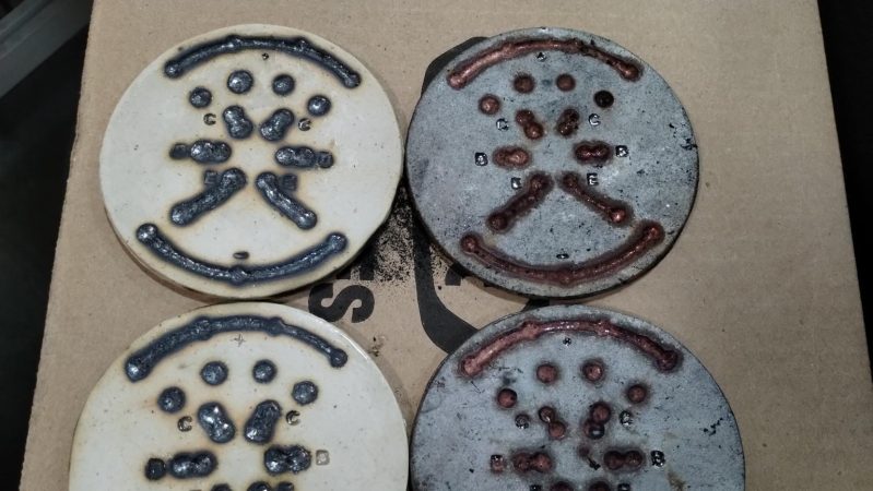
Solarpunk is all about combining that DIY hacker ethos with sustainability and renewable resources. Our usual PCB manufacturing methods, with their bevy of chemical baths and petrochemical resins aren’t exactly the most sustainable. Digging up some clay and firing it into a circuit board? Very sustainable! And apparently doable, as demonstrated by [Emily Velasco] on Mastadon.
Of course anybody could take a ceramic wafer and call it a circuit board, but that’s only part of what [Emily] did. The ceramic wafer is apparently native clay, which is very cool. Even cooler is that she’s baked the traces into the pottery. While you could conceivably use some sort of conductive glaze for this, what [Emily] did was stamp her desired circuit into the unfired ceramic using a 3D-printed stamp, and then fill the depression with copper powder after the first firing. After that, a second firing is done in a reducing atmosphere to melt/sinter the copper together–it’s not totally clear which is happening here–without burning up.
The results speak for themselves; on the finished demo board, a pair of LEDs blink happily away, driven by the astable oscillator circuit baked right into the clay– and of course the components soldered to it. You’ll have to click through to see it, though.
Given those not-so-sustainable petrochemicals behind our favourite PCBs may be in short supply, this is a timely hack. If it seems familiar, that’s because we featured virtually the same technique last year, but using more-expensive silver powder instead of copper, and a campfire instead of a kiln.
Thanks to [smellsofbikes] for the tip!


For IBM’s mainframe thermal conduction modules, which were many-layer ceramic pcbs with shrinkage controlled precisely enough the chips could be mounted directly to them, the solution was to use molybdenum paste to print the traces since it would sinter at the same range of temperatures that the ceramic did.
(TCMs started fading out of use as the company switched from bipolar to CMOS.)
I was thinking. Molybdenum has a melting point of 2620 degrees Celcius. A ‘normal’ ceramics kiln goes up to some 1200 degrees Celsius, way too low for Molybdenum to melt together.
Aluminium powder has a melting point of about 661 degrees Celsius, while copper powder melts at around 1085 degrees Celsius. So there’s a good chance that the Copper powder actually did melt, in this example. But it doesn’t look very good, to be honest.
But there’s also Aluminium. Aluminium has a lower conductivity, but still quite enough for most electronics I would say. But it can be solidly molten in any kiln, and so might come out better than copper.
But Aluminium has an issue: it oxidizes like crazy, so is hard to solder. However, if you apply some mineral oil and scrape the oxide away under it, you can solder it. And it sticks quite well. You do need quite some heat because Aluminium is a great heat conductor. But the traces are small, so should not be too hard to heat up. https://hackaday.com/2022/03/06/how-to-solder-to-aluminum-easily/
So, you could try using Aluminium powder, which would surely melt in a normal kiln. And then use the oil-scrape-solder method to solder the components to it.
But thinking about it further… I wonder if you could fill the gaps in the ceramic with aluminium powder, and put a small blob of lead/tin solder at the points where you want to solder stuff. Then fire it at maybe 700 degrees Celsius so that the aluminium powder melts together AND bonds to the lead/tin blobs at the same time.
That might give you a better looking pcb than when using copper, but is just as easy to solder the components to.
Thinking about it even further. I wonder how the copper is kept sticking to the ceramics? Are the traces easy to pull off?
Maybe mix something into the copper that has the same melting temperature as the copper, actually bonds with the ceramics substrate, and holds the copper stuck to the substrate?
Replying to myself. :P The answer is in one of her Mastodon posts.
“I just mixed copper powder into some of the basic glazes we have at the studio, like clear and green celadon. There are actualy copper glazes that people use in raku firing though. You can find recipes online”
Also: even having a (slightly) reducing atmosphere prevents the bulk of the copper from ixidizing, but the remaining copper oxide tends to bond to the ceramic, even aluminium oxide (alumina).
If the metals melt at the same time as aluminum they will mix, particularly in the timefranes involved in kilns. Not sure what pb-al amalgam looks like but I wouldn’t be surprised if it’s useless. See also – what happens when mercury is poured on aluminum
Hi!
Molybdenum is commonly blended with manganese and fired under partial pressure hydrogen atmosphere. Also it is more of a co-sintering versus a proper melting of the metals.
In some cases this approach is very much still used, either in ceramics or for spatial/military use where water vapour or other gases (Helium?) have to be preventet from penetrating the chips or MEMs.
Odds are covering the board with sodium borate before firing would not only produce better results but possibly allow regular oxygen firing as long as it’s not too long. Then soaking the board in water would dissolve the Flux leaving behind copper. Idk honestly how long they fired it for.
Hi,
the borate will also begin to react with the clay-wafer and form a low melting low viscosity glaze. Maybe this is good, maybe not. One could also use boric acid instead, which sontains next to no sodium which you might want to limit Na in some cases.
(I’ve done some glass and glaze recepies during at the engineering school: you have to watch viscosity, thermal expansion, solubility, toxicity, melting interval, opakeness/translucency out-gassing etc. more or less at the same time.)
I worked at Delco Electronics for years, where we made hybrid circuits with ceramic (Al2O3) substrates. They were very heat and vibration-tolerant; they could be mounted directly to the engine. The substrates were made by Coors, the beer people, they also make ceramics. Copper-based traces turned into a disaster in production, they worked OK in small quantities. The arc seies of radios used them, we didn’t dare try again after that.
I love this idea. Imagine having a flower pot that you plug into a wall and it charges your phone.
I could see glass, aluminum, paper, etc in a post scarcity world as substitutes. Might even be easier to work with.
Hit your ceramic substrate with a fine hydrogen ion jet and you can reduce it locally to metal.
Yes, but potassium, calcium, magnesium and sodium are very reactive, silicon is barely a metal and aluminium would most probably resist all attempts to be reduced to metal. – There is a reason to use costly elctricity instead of just using hydrogen to produce aluminium. Also the reaction mechanics dont’ pan out, IIRC my chemistry classes. But maybe there are new technologies i’ve never heard of.
Other non-silicious substrate could be more advisable for that apporach. Also removing all the oxygen would result in a significant shinkage which would expose the conductive path to the point it would loose grip on the substrate, a bit like a hotdog in its bread roll…
Interesting! I wonder how well the traces stick, and also what the dielectric constant looks like for generic clay
It’s bad.
For frequencies above 100Hz, soapstone-ceramics (HF-statite) that were developped in the first years of RADAR and radiobraodcasting are better. The best are plastics, followed amorphous silica, sapphire and engineered ceramics as pure alumina, aluminium nitride, etc.
Lots of talk about Aluminum here, but I don’t see much about ceramics. The first super conductor was a special ceramic, YBO, I think. It makes me think about Aluminum being naturally anti-magnetic. Expecting succes when chilling the metal and board to superconductor temperature without breakage feels naive. But, if successful, what would you expect from antimagnetic traces inside a superconductor?