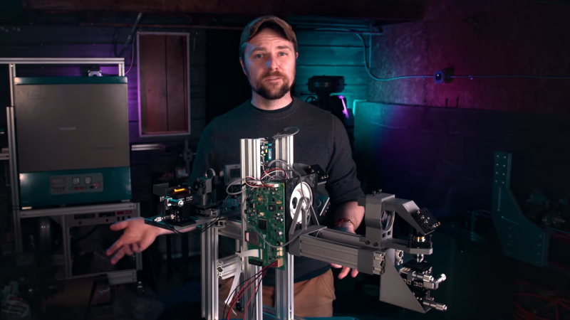
What does it take to make your own integrated circuits at home? It’s a question that relatively few intrepid hackers have tried to answer, and the answer is usually something along the lines of “a lot of second-hand equipment.” But it doesn’t all have to be cast-offs from a semiconductor fab, as [Zachary Tong] shows us with his homebrew direct laser lithography setup.
Most of us are familiar with masked photolithography thanks to the age-old process of making PCBs using photoresist — a copper-clad board is treated with a photopolymer, a mask containing the traces to be etched is applied, and the board is exposed to UV light, which selectively hardens the resist layer before etching. [Zach] explores a variation on that theme — maskless photolithography — as well as scaling it down considerably with this rig. An optical bench focuses and directs a UV laser into a galvanometer that was salvaged from an old laser printer. The galvo controls the position of the collimated laser beam very precisely before focusing it on a microscope that greatly narrows its field. The laser dances over the surface of a silicon wafer covered with photoresist, where it etches away the resist, making the silicon ready for etching and further processing.
Being made as it is from salvaged components, aluminum extrusion, and 3D-printed parts, [Zach]’s setup is far from optimal. But he was able to get some pretty impressive results, with features down to 7 microns. There’s plenty of room for optimization, of course, including better galvanometers and a less ad hoc optical setup, but we’re keen to see where this goes. [Zach] says one of his goals is homebrew microelectromechanical systems (MEMS), so we’re looking forward to that.


Perfect for storing bitcoin private keys
The Zeloof Z2 had 10-micron features. He fit 100 NFETS in 2.4mm2, and definitely had room for a ton of optimization for that process, though he’s already moving on to his next process. I’d bet you could easily get an order of magnitude improvement with the same process, which would give ~400transistors/mm.
As he notes, the 4004 had 2200 transistors. A real ballpark estimate of a small risc-v implementation would be 12,000 transistors, based off of a 2-transistor NAND, vexriscV and Xilinx app note 59. I could be way off there. Assuming another 20% gates for supporting logic, IO, etc (probably a low assumption), we’d be at 15k. Assuming that’s a reasonable first-order approximation, we would get 37mm2 for just the processor logic, or a square die with 6mm sides.
Thus, after an exhausting chain of possibly ridiculous assumptions, you could maybe use this laser lithography machine to etch yourself a reasonably-sized, low-performance risc-v microcontroller. And that’s all assuming that this lithography machine is well suited to the process Zeloof was using. I’m very far from an expert on the matter, so that fundamental assumption could easily be wrong.
https://hackaday.com/2021/08/14/the-zeloof-z2-intergrated-circuit-has-100-transistors/
After watching the video, I think the machine would be applicable to the same process, but it would need a lot of tuning and improvement before doing so. I look forward to his updates.
Now it is just the rest of the setup left.
A lithograph is about as far into semiconductor/MEMS manufacturing as a few lone train axels are a train.
Ie, putting a pattern into resist is just one part of the overall puzzle.
Putting down an even layer of resist without wobbles in the surface can sometimes be a tricky enough challenge. (all though, a hard drive spindel is usually a decent source for a near perfect bearing, and an HDD spindle comes with a sufficient motor as well.)
Then there is depositing materials and having them adhere correctly.
Avoiding trapping dust, or sometimes even stray gas.
Etching is its own can of worms to contend with to not under or over etch features. Or even get an even etching.
We also have material choices to make, not everything will play nicely at all times, and contamination is a huge issue if one aims for semiconductors. (also, avoid copper, silicone junctions considers it poison as it turns transistors into resistors, and it also etches like junk down these sizes. (ie, it etches really unevenly, there is reasons the industry has etching assisted polishing and not just etching alone for this process.))
And lastly, the most important thing!
Layer alignment.
It doesn’t matter if you nailed everything above perfectly if your different features are 10’s of µm away from where they should be relative to each other. Also, just going with “absolute” alignment to a reference surface is usually not sufficient, dust, grease, and surface variations in your substrate can make major offsets, not to mention clamping force and temperature. (optical alignment to reference markers in the previous layers is usually the safest bet. (since it can usually aid with solving the bellow as well.))
And for alignment, we don’t just have to consider X and Y, but also rotation in 3 axis and variations in scaling (“zoom”), focus also plays a role.
In short.
I personally don’t find it impressive to etch nor deposit any material at a microscopic size.
Align to layers within a few µm from each other is a lot more impressive, especially if the other processes are reasonably made as well.
… a really long winded way of saying you only care about the end result and not the journey. Sure an axle doesn’t make a train but a train is not a train without first having axles either. Loosen up a little and try not to dismiss the intermediate steps just because someone’s hobby is not already polished and done to your exact standards.
I have seen people build “lithography systems” over and over and over. It is the first thing most people tackle when going for chips or MEMS, only to then give up when faced with alignment, etching quality, or just getting a deposited material to stick. And then they haven’t even started exploring dopants.
My comment is more about what to face next.
The lithograph is an important tool, but it is only a single step on an otherwise long journey.
I want to see more people than just Zeloof manage to build a decent DIY chip. But that requires that people stop considering the lithograph as this “major step”, since it isn’t.
If one makes a transistor with 500nm features or 5mm features doesn’t largely matter, it is roughly equally hard to get a decent result. Scaling it down makes it more sensitive to dust. But general contamination is a major concern regardless, and adjusting the dopings to alter the transistor’s properties is still informative.
Making things microscopic isn’t all that important. One will fit more in a given area if the features are smaller, but getting the features to start with is a decent first step, even if they are huge. And doing it at the mm size takes away some of the issues of microscopic sizes and largely removes the hardest part that is alignment.
If one can build a working transistor and perhaps even make some metal interconnects on the mm size with manual alignment, then when one builds the lithograph with optical alignment, one won’t have to adapt one’s process much to get a working chip once more, but at a much smaller size.
To link back some 12 years.
Here is a guide to making semiconductors in the typical kitchen oven: https://hackaday.com/2010/05/13/transistor-fabrication-so-simple-a-child-can-do-it/
He has been actively exploring doping, it’s the next video back on his channel.
Then I will have to say he is further than most.
Since a lot of projects I have seen throughout the years just fiddles with the lithograph and crudely etching copper, before giving up when they can’t etch sub 10µm wide traces without the etchant eating through at random points. (this were one of the problems holding back copper interconnects all the way until the 90’s. The other thing holding it back were finding a suitable diffusion barrier to slow down the copper diffusing into the semiconductors.)
Aluminium apparently etches a lot more evenly. And it isn’t toxic to semiconductors since it forms a light P dopant in silicon. (though, usually one uses tungsten to form the terminals onto the semiconductors, since tungsten doesn’t care about moving about, so it doesn’t for a depletion region unlike aluminium.)
Then you could just say that, instead of inserting yourself and what you do or don’t find impressive (that’s completely irrelevant, and just makes you sound arrogant). No point pinning what you see other people doing/not doing on this specific creator. Just provide your suggestions without the “I” or “but other people aren’t even doing X or are doing Y which I consider wrong”.
I’m pretty sure ‘Concise’ isn’t in Wikstrom’s vocabulary. I’ve never seen any posts from him that weren’t long-winded and borderline incoherent.
I think his message gives important context and guidance useful to readers contemplating doing something similar. Much appreciated.
> I personally don’t find it impressive to etch nor deposit any material at a microscopic size.
then keep it to yourself. the guy didn’t exaggerate anything. he just told us what his goal was.
And I just love to watch his videos (and his skills!) getting better and better. His presentation style and especially his calmness is a treat in modern Youtube times.
Regarding Alexander Wikström’s post: Yeah, your post is the perfect example for a discouraging, not-at-all helpful kind of “rant”.
I hope he’s above that kind of rambling and keeps following his journey!!!
My expression is more in regards to the general statement that “oh it is a lithograph, now make chips!” that so many people tend to have with a complete disregard to the rest of the process.
I am not dismissing the project, nor the creator of it. He has actually gotten some decent results, but I think he should tackle alignment next. And that he still has a long way to go before MEMS is a possibility.
Though, he has given himself an interesting challenge by using a galvanometer instead of the typical UV projector.
I have seen Hack a day feature people a few times that has built a lithograph or etched some crude lines in copper foil and gotten 20µm pitch. Only for those projects to grind to a halt over “unforeseen” difficulties. Usually alignment, etching quality, adherence of deposited layers or just contamination (though few seems to get this far). (or simply running out of founds for what they thought were a “simple” project.)
Don’t bother explaining to someone, that only expectation is pat on the back. Setup some RSS, have piece of mind, recall times when there was something called constructive criticism.
I have noticed how constructive criticism at times isn’t appreciated by a lot of people.
When it comes to semiconductors a lot of people just focus on going small, even though it really isn’t important.
MEMS however is a different story.
The smaller sizes allows for a lot more interesting things. Mostly since a given aspect ratio can be kept in a part while its weight drastically reduces as one goes down in size. Effectively it is the square cube law at play and a lot of MEMS stuff simply couldn’t be built above the mm feature size.
And since Zach stated he is interested in MEMS, and why I emphasized the post on the importance of alignment.
Since for semiconductor stuff, we can just work at a larger feature size were we can align properly, but this isn’t as easily done with MEMS. So focusing on getting good alignment and then getting good etching and depositioning after we have established adequate alignment for the part we desire to make.
High aspect ratio etching can also be a can of worms worth exploring. And here there is a few interesting paths, either Ion bombardment, laser drilling/cutting, or just coating the inner diameter of the hole/trench in resist and only exposing the very bottom of it (or just the walls if having a negative resist), the last option though requires a fairly insane alignment accuracy compared to the feature size.
Though, comparing alignment requirements for semiconductor and MEMS is interesting.
For semiconductors almost all textbooks talks about 2:1, ie want to make a 2µm feature, then you need a 1µm accuracy in the alignment (1µm total for all axis of movement, rotation and scale). But a lot of MEMS stuff I have read talks about 5:1, or even 20:1. (ie, want to make features at 2µm, then you might need 100nm alignment accuracy) Meanwhile some semiconductor stuff can talk about 3-4:1 for more yield sensitive stuff, or just analog/RF.
But the thing that makes alignment hard is that here we talk about being inside that spec for the whole working area, not just at a point. And when we start thinking of that things just gets insane.
Lets say we need a chip with 50 nm features, then we need to align this within +/-25nm. If we on one side of the chip are off with 25 nm and on the other side of the chip is 25nm off in the other direction. That gives us a total error of 50nm, the exposure is a bit incorrectly scaled but no biggie. Except, that can be 50nm across a 10×10 mm chip. If scaled along the diagonal it is only 0.00035% (3.5ppm) incorrectly scaled and that is the worst that we accept when having a generous spec of 2:1. (technically when just incorrectly scaled in 1 axis the worse here would be 5ppm)
Fine line between constructive criticism and being unconstructively dismissive that a lot of people unintentionally cross. But whether it’s intentional or not it still deserves being called out. That’s my constructive criticism to people who find themselves on the wrong side of that line!
“i’m not impressed” isn’t criticism, constructive or otherwise. it’s just rudeness.
the rest of the comment was perfectly useful, and ruined by an apparent need to dismiss the work because of irrational exuberance on the part of people besides the video creator.
Ditch the galvos. Use a DLP chip instead. No more scanning issues.
What would be neat is using the rotating, multi-sided mirror from something like a LaserJet III to scan a controlled pulse LASER for vat of resin stereolithography 3D printing. The rotation scans across the build surface and have a traverse mechanism to move across the other axis line by line. Resolution would be dependent on how tight the beam can focus, how fast it can be pulsed, and the resolution of the traverse mechanism. Might also want variable focus to control spot size VS mirror rotation angle to account for the change of beam angle where it meets the resin surface.
Or did those printers have additional optics to change the beam angle where it met the OPC drum so it didn’t have fatter dots toward the edges? Or was the progressive ovalization towards the edges not considered an issue with printing onto paper?
As Zach notes, one of the nice things about this galvo setup is that it takes gcode input, which really reduces the work required to get stuff going.
I achieved the same results on a dvd drive